Semiconductor device using multi-layer unleaded metal plating, and method of manufacturing the same

a technology of unleaded metal and semiconductors, which is applied in the direction of semiconductor devices, semiconductor/solid-state device details, electrical equipment, etc., can solve the problems of whisker resistance left behind, the anxiety of the influence of lead or lead alloy on the human body, and the problem of groundwater contamination, etc., to achieve the effect of reducing the area of the crevice between the particles, reducing the absolute quantity of residual stress between the particles, and improving whisker resistan

Inactive Publication Date: 2006-04-06
SOCIONEXT INC
View PDF0 Cites 16 Cited by
  • Summary
  • Abstract
  • Description
  • Claims
  • Application Information

AI Technical Summary

Benefits of technology

[0043] In the inner layer, the fine metal-plating grain is created, and the adhesion to the base material of the external connection terminal can be secured. In the surface layer, the coarse grain is created, and the whisker resistance can be improved by the coarse-grain metal plating layer of the surface layer.
[0044] One major factor of the whisker is the residual stress between the particles at the time of metal plating, and the absolute quantity of the residual stress between the particles can be decreased by forming the surface layer with the metal-plating coat of the coarse grain. In addition, if the surface layer of the coarse grain is formed, the area of the crevice between the particles can be decreased, which serves in favor of the heat resistance and the moisture resistance, and the solder wettability over an extended period of time can be kept good.

Problems solved by technology

However, in recent years, from the viewpoint of earth environment protection, there is the outstanding anxiety about the influence of the toxicity of lead or lead alloys on the human body, especially the groundwater contamination.
The 100% tin metal plating is already put in practical use but it has the problem of whisker resistance left behind.
There is the possibility that it becomes a serious problem.
However, the occurrence mechanism of whisker is not solved completely, but they are merely the results of the experiments and still cannot be put in practical use.
The shortcoming of the tin-bismuth alloy metal plating is the characteristics of bismuth which makes this alloy metal hard and brittle, and it causes the occurrence of cracks of the metal-plating coat due to the bending of the external terminals of the semiconductor device as well as the lowering of the solder bonding strength after the secondary mounting.
However, because of the above-mentioned shortcoming, it is difficult to raise the content ratio of bismuth of the tin-bismuth alloy metal plating so much.
The shortcoming of the tin-silver alloy metal plating is that the metal-plating coat is easy to corrode, which causes the problems, such as discoloration of the metal plating and migration.
Furthermore, the tin-silver alloy metal plating has also some problems that its whisker resistance is inferior to that of the tin-bismuth alloy metal plating, and that the solder wettability falls due to the inclusion of silver therein.
Moreover, also except functionality, the stability of the metal-plating liquid is poor, which causes the problem that the running cost including the metal-plating liquid adjustment etc. becomes very high.
The environment where the tin-silver alloy metal plating can be used is limited, and the cost becomes high.
However, since the reliability after the secondary mounting is comparatively good, the tin-silver alloy metal plating is used in many cases in the environment where the tin-bismuth alloy metal plating cannot be used.
But the shortcoming of the tin-copper alloy metal plating is that it has a low whisker resistance and a poor solder wettability.
Especially, the environment where the tin-copper alloy metal plating can be used is limited.
Furthermore, there is also the problem in that any technique which measures the metal-plating coat composition and thickness on the copper material in non-destructive manner is not established.
However, the numerical value is extremely low, the management of the content ratio of copper is very difficult.
In addition, it is the limit also as measuring instrument accuracy, and managing as the product warranties is hardly carried out for the practical use.
Moreover, in the latest report, degradation of the tin-copper plating liquid is severe, and the adjustment by the supplement cannot be performed.
As long as the cost in the long run is concerned, it cannot be said that the expense is cheap.
It is difficult to overcome the problems, such as the occurrence of cracks of the metal-plating coat due to the bending of the external terminals of the semiconductor device as well as the lowering of the solder bonding strength after the secondary mounting.

Method used


Image

  • Semiconductor device using multi-layer unleaded metal plating, and method of manufacturing the same
  • Semiconductor device using multi-layer unleaded metal plating, and method of manufacturing the same
  • Semiconductor device using multi-layer unleaded metal plating, and method of manufacturing the same

Examples


Embodiment Construction

[0056] A description will now be given of the preferred embodiments of the present invention with reference to the accompanying drawings.

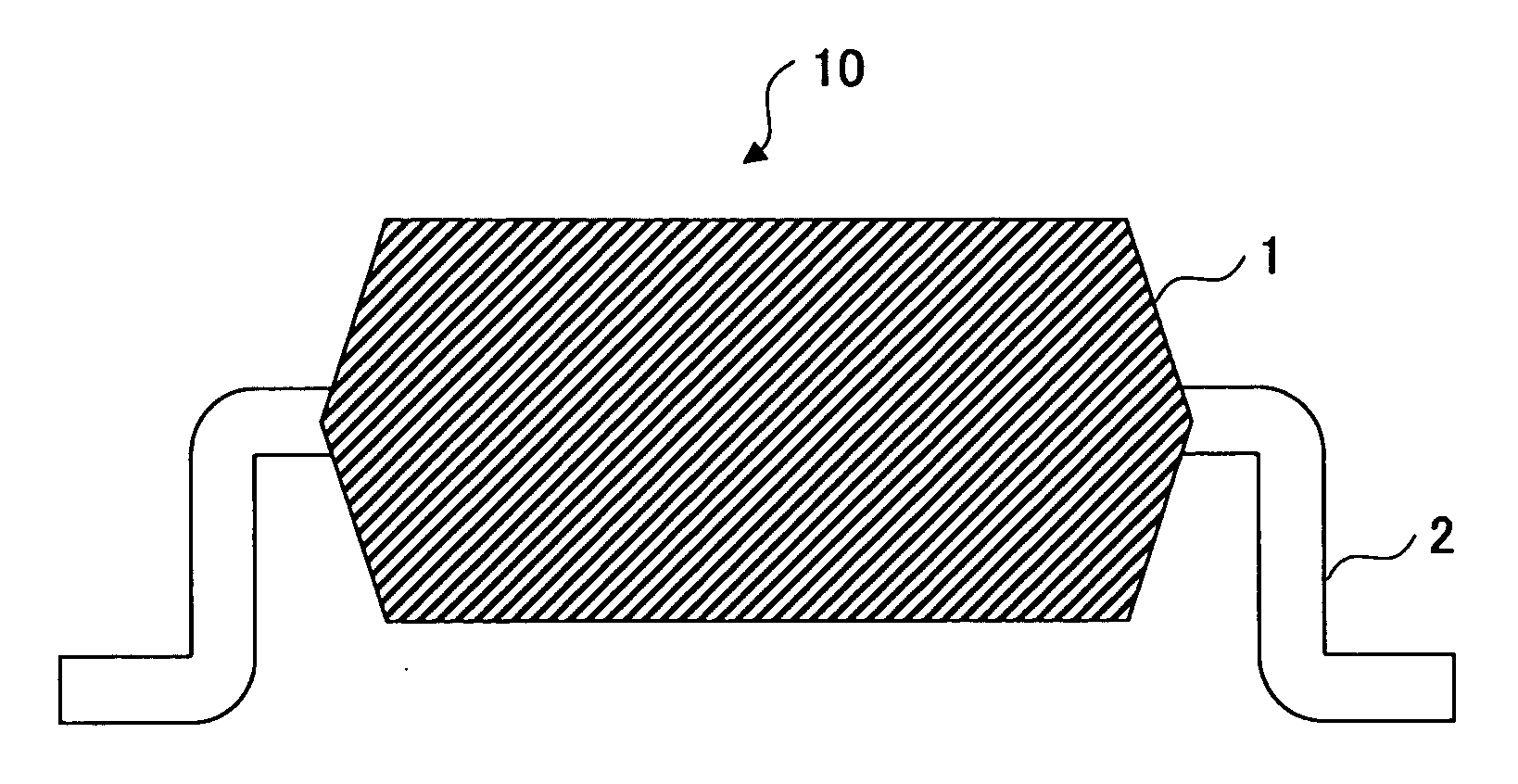
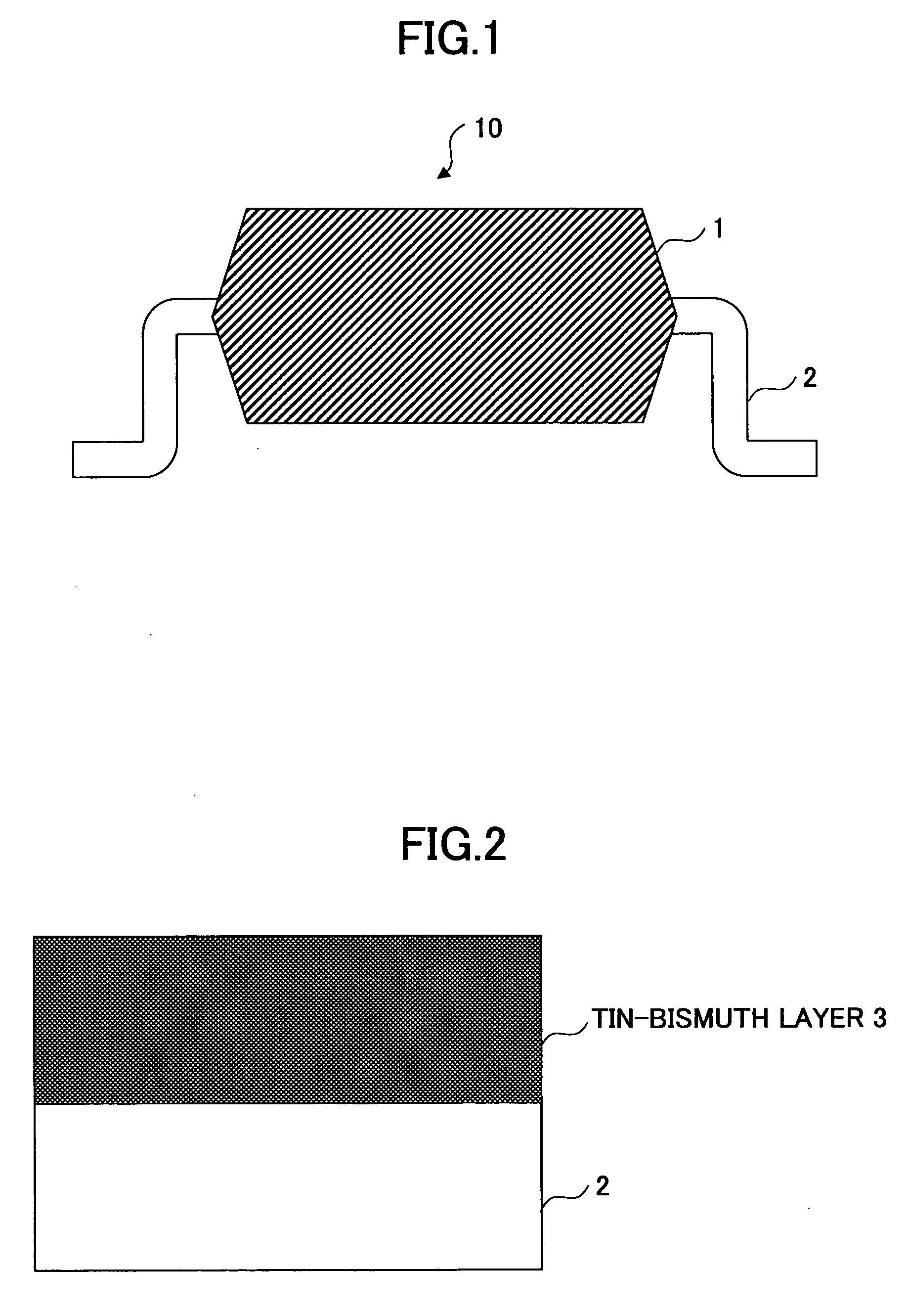
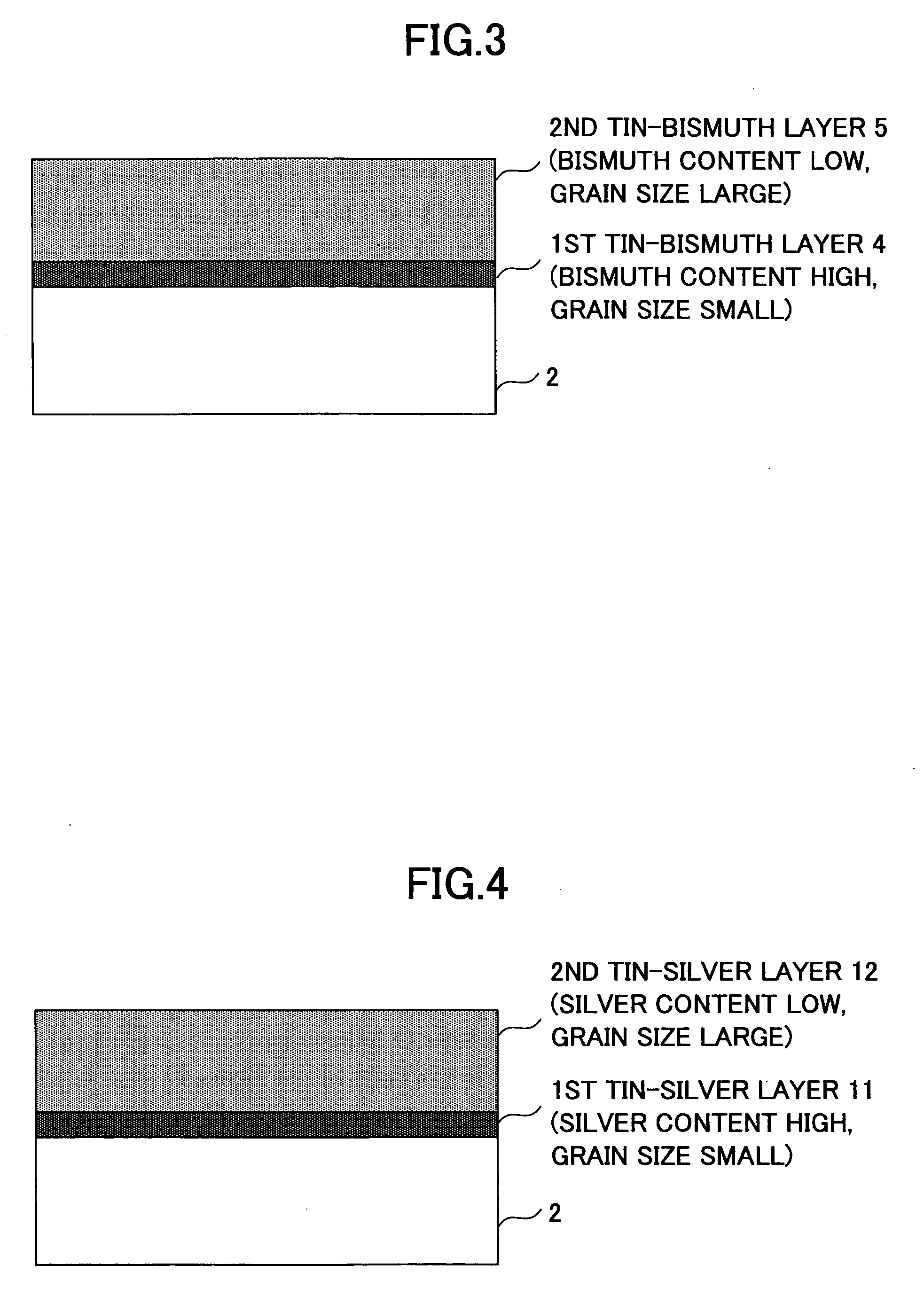
[0057]FIG. 1 shows the composition of a semiconductor integrated circuit device in which the semiconductor device according to the invention is embodied. FIG. 3 is a cross-sectional view showing the composition of an example of the multi-layer unleaded metal plating layers formed on the lead of the semiconductor integrated circuit device of FIG. 1 using the multi-layer unleaded metal-plating method in the first preferred embodiment of the invention.

[0058] The multi-layer unleaded metal-plating method of the present embodiment is the method which forms the two different unleaded tin-alloy plating layers (which is inclusive of a 100% tin plating layer) on the base material of the lead as the inner layer and the surface layer.

[0059] The semiconductor integrated circuit device 10 of FIG. 1 comprises the IC package 1, and the lead 2 which is an exter...


PUM

PropertyMeasurementUnit
grain sizeaaaaaaaaaa
thicknessaaaaaaaaaa

Abstract

A semiconductor device comprises a semiconductor integrated circuit, an external connection terminal connecting the semiconductor integrated circuit to an external device, and a plurality of tin or tin-alloy plating layers formed on the external connection terminal as multiple unleaded metal plating layers. The multiple unleaded metal plating layers comprise a first layer made of a tin alloy and provided as an inner layer of the multiple unleaded metal plating layers, the tin alloy of the first layer containing as a second element one of bismuth, silver, copper, indium, and zinc, and a second layer made of either 100% tin or a tin alloy and provided as an outer surface layer of the multiple unleaded metal plating layers, the 100% tin or the tin alloy of the second layer having a percentage of tin content greater than that of the first layer.

Description

CROSS-REFERENCE TO RELATED APPLICATIONS [0001] This application is based upon and claims the benefit of priority of Japanese Patent Application No. 2004-282234, filed on Sep. 28, 2004, the entire contents of which are herein incorporated by reference. BACKGROUND OF THE INVENTION [0002] 1. Field of the Invention [0003] The present invention relates to a semiconductor device having an external connection terminal formed with multi-layer unleaded metal plating, and a method of manufacturing the semiconductor device. [0004] 2. Description of the Related Art [0005] Soldering is the widely used bonding method of electrically and mechanically connecting a semiconductor device to a printed circuit board. [0006] In order to make connection with the solder easier, tin or tin-alloy plating is usually formed on the external connection terminal of the semiconductor device. [0007] Most frequently used one among such alloy plating is tin-lead alloy plating, and the tin-lead alloy plating has excel...

Claims


Application Information

Patent Timeline
Patent Type & Authority Applications(United States)
IPC IPC(8): H01L23/48H01L23/52
CPCH01L23/49582H01L2924/00014H01L2924/01322H01L2224/45099H01L2924/0002H01L2924/00
Inventor KOTAKI, YOSHITSUGUKANAZAWA, YUUKI
Owner SOCIONEXT INC
Why Eureka
Try Eureka