Polymer encapsulated dicing lane (PEDL) technology for Cu/low/ultra-low k devices

a technology of polymer encapsulation and dicing lane, which is applied in the direction of semiconductor devices, semiconductor/solid-state device details, electrical apparatus, etc., can solve the problems of reducing capacitance, reducing mechanical and thermal stability, and presenting yield and reliability vulnerabilities of semiconductor devices

Inactive Publication Date: 2006-04-13
AGENCY FOR SCI TECH & RES
View PDF3 Cites 57 Cited by
  • Summary
  • Abstract
  • Description
  • Claims
  • Application Information

AI Technical Summary

Problems solved by technology

The presence of low k layers, resulting in decreased capacitance, however inherently presents lower mechanical and thermal stability than the higher k, silicon oxide layers.
Therefore low k layers present in semiconductor devices can present yield as well as reliability vulnerabilities in terms of interfacial delamination and cracking which can occur in the low k layers as a result of subsequent semiconductor device or packing procedures.
For example the flip chip process of connecting solder balls or bumps of a semiconductor chip to an underlying package, as well as the dicing procedure used to separate individual semiconductor chips from a completed semiconductor substrate, can result in undesirable phenomena such as adhesion losses between copper and the low k layer, as well as micro-cracking of these same materials.
To enhance the mechanical strength of these materials undoped silica glass (USG) layers have been formed on the underlying low k layers and copper interconnect structures allowing these structures to more adequately survive subsequent processing procedures, however the presence of the higher k, USG layers increase parasitic capacitance thus reducing the performance benefit derived with the use of low k layers.

Method used


Image

  • Polymer encapsulated dicing lane (PEDL) technology for Cu/low/ultra-low k devices
  • Polymer encapsulated dicing lane (PEDL) technology for Cu/low/ultra-low k devices
  • Polymer encapsulated dicing lane (PEDL) technology for Cu/low/ultra-low k devices

Examples


Embodiment Construction

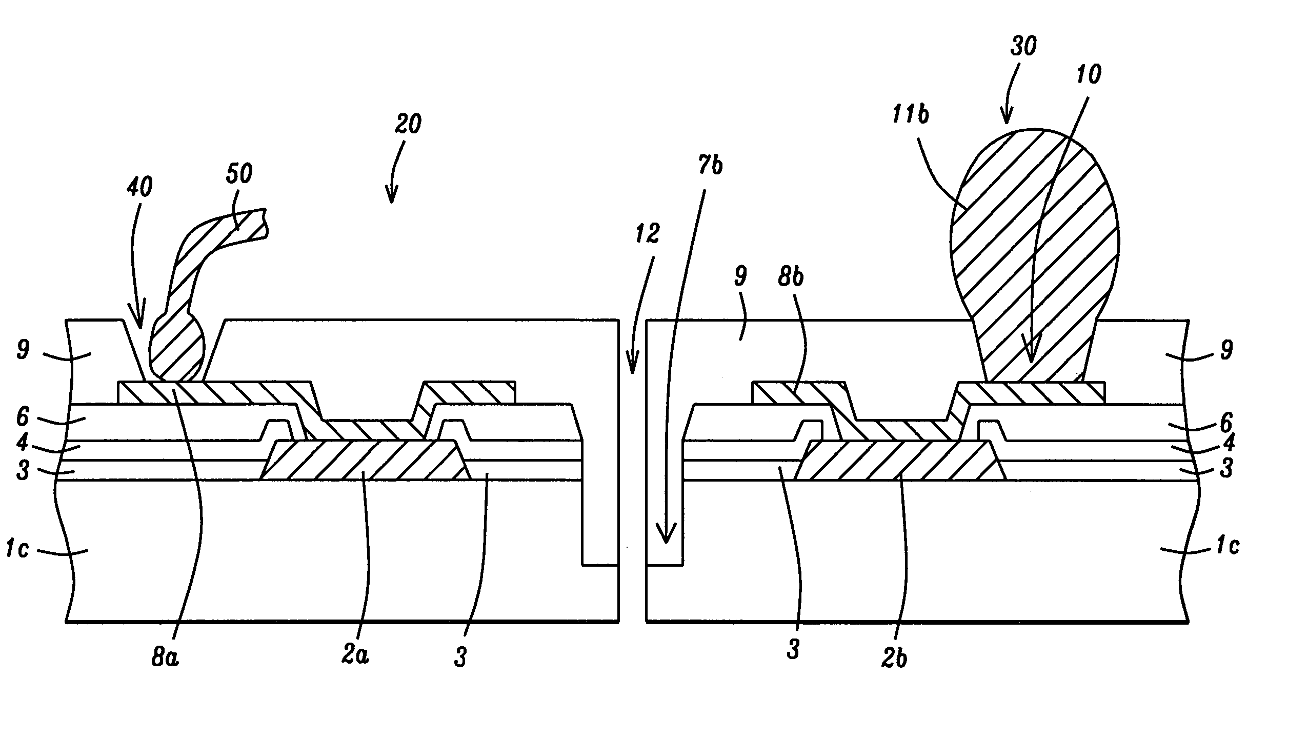
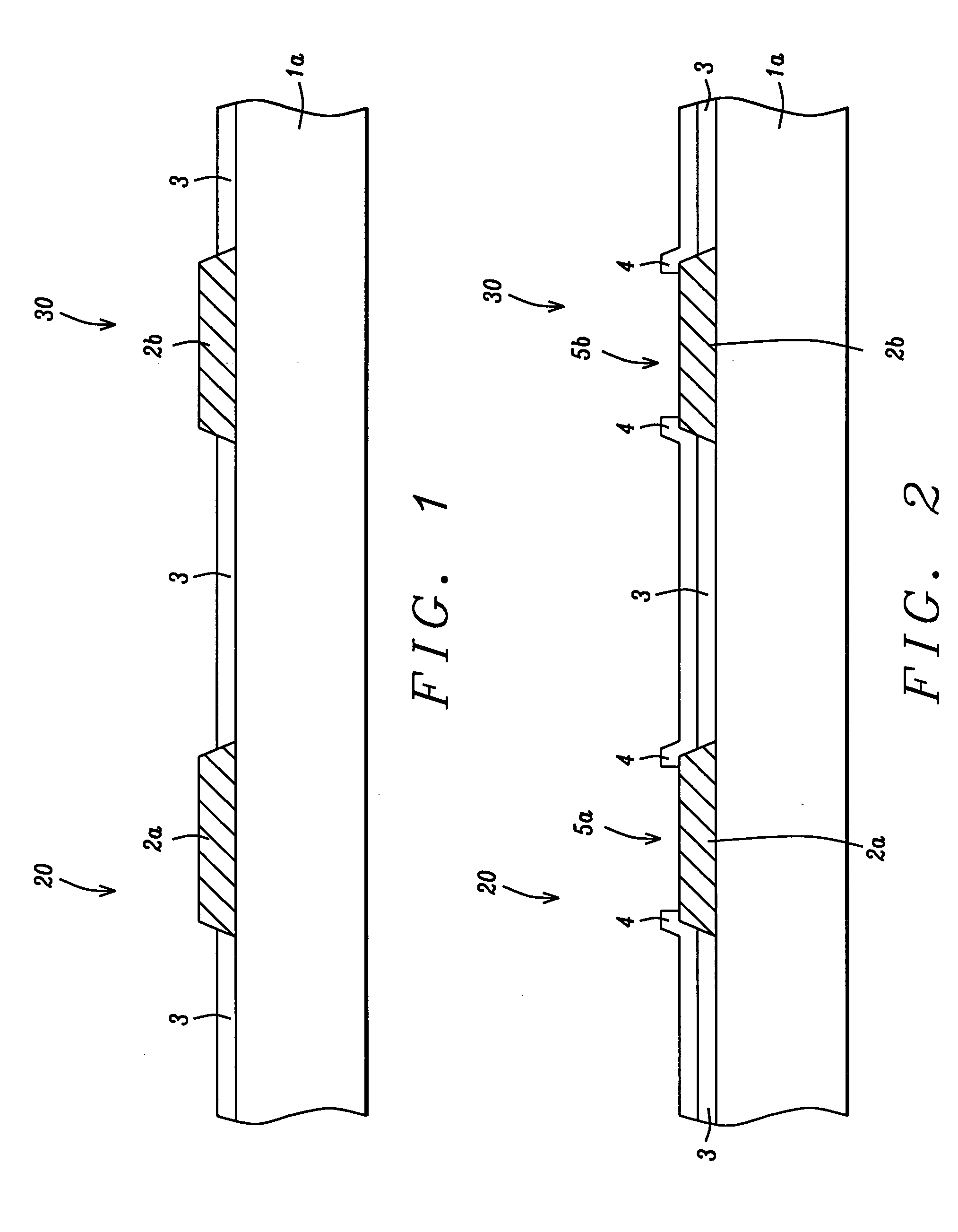
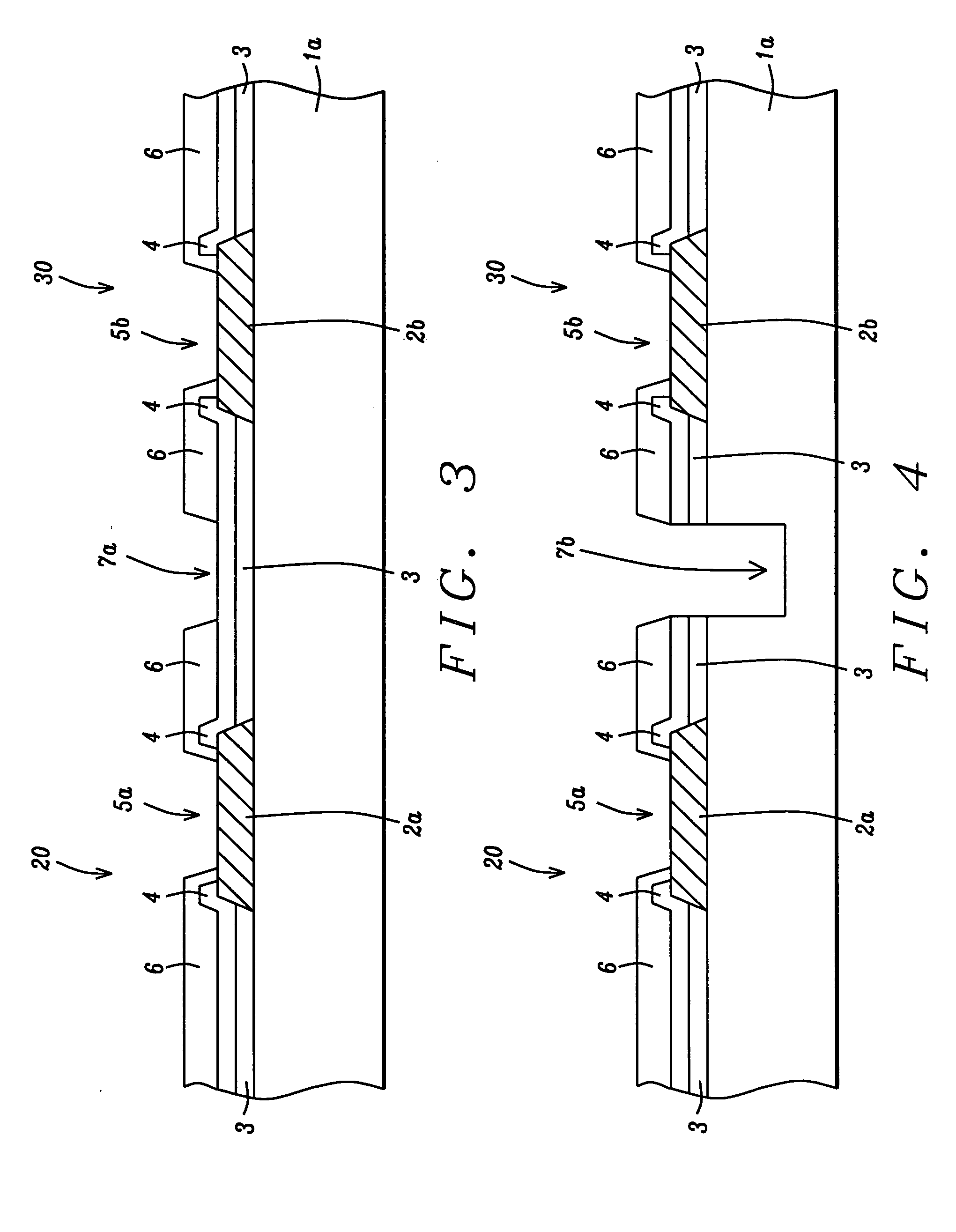
[0012] The method of fabricating a semiconductor device comprised with copper interconnect structures and low k layers featuring polymer encapsulation layers used to protect the key components of the semiconductor device during specific processing steps such as dicing, will now be described in detail. Semiconductor substrate 1, which will be used to provide the final diced chips, is schematically shown in FIG. 1. Semiconductor substrate 1, is comprised with the necessary micro-electronic elements, (not shown in the drawings), such as metal oxide semiconductor field effect transistor (MOSFET) devices, resistors, and capacitors. These elements formed via front end of the line (FEOL), as well as back end of the line (BEOL), processes, are either embedded in, or located on the top surface of semiconductor substrate 1. Portion 20, of semiconductor substrate 1, will be used to fabricate devices which will require wire bonding for subsequent external connection, while portion 30, of semico...


PUM

PropertyMeasurementUnit
thicknessaaaaaaaaaa
thicknessaaaaaaaaaa
dielectric constantaaaaaaaaaa

Abstract

A process for packaging semiconductor devices for flip chip and wire bond applications, wherein specific materials of the semiconductor devices are protected during device processing sequences and dicing procedures, has been developed. After definition of copper interconnect structures surrounded by a low k insulator layer, a protective, first photosensitive polymer layer comprised with a low dielectric constant is applied. After definition of openings in the first photosensitive polymer layer exposing portions of the top surface of the copper interconnect structures, a dicing lane opening is defined in materials located between copper interconnect structures. Conductive redistribution shapes are formed on the copper interconnect structures exposed in the openings in the first photosensitive polymer layer, followed by application of a protective, second photosensitive polymer layer. An opening is defined in the second photosensitive polymer layer exposing a portion of the top surface of a redistribution shape followed by placement of a solder ball in this opening. A reflow anneal procedure results in the solder ball wetting and overlying only the portion of the redistribution shape exposed in the opening in the second photosensitive polymer layer. Separation of the solder ball, flip chip regions from the non-solder ball, wire bond regions is accomplished via a dicing procedure performed in the dicing lane.

Description

BACKGROUND OF THE INVENTION [0001] (1) Field of the Invention [0002] The present invention relates to methods used to fabricate semiconductor devices and packages, and more specifically to a method used to protect the copper interconnects and low dielectric constant (low k) materials of the semiconductor device during subsequent dicing, interconnection processes and further packaging procedures. [0003] (2) Description of Prior Art [0004] To increase semiconductor device performance or to decrease resistance—capacitances (RC) delay the semiconductor industry has been employing copper as an interconnect material replacing more resistant aluminum based structures, while employing dielectric layers with a lower dielectric constant than silicon oxide to replace higher dielectric constant materials. The presence of low k layers, resulting in decreased capacitance, however inherently presents lower mechanical and thermal stability than the higher k, silicon oxide layers. Therefore low k la...

Claims


Application Information

Patent Timeline
Patent Type & Authority Applications(United States)
IPC IPC(8): H01L21/44
CPCH01L2224/0401H01L2924/01024H01L2224/1148H01L2224/13099H01L2224/131H01L2224/45144H01L2224/48463H01L2924/01003H01L2924/01013H01L2924/01014H01L2924/01022H01L2924/01028H01L2924/01029H01L2924/0105H01L2924/01057H01L2924/01073H01L2924/01075H01L2924/01078H01L2924/01079H01L2924/01082H01L2924/014H01L2924/04953H01L2924/13091H01L2924/19041H01L2924/19043H01L2924/30105H01L2224/05556H01L2924/01019H01L2924/01006H01L2224/13022H01L2924/0002H01L2924/1306H01L2224/04042H01L2224/02166H01L2224/48599H01L23/3185H01L23/3192H01L24/05H01L24/11H01L24/12H01L24/73H01L2224/0231H01L24/48H01L2224/05548H01L2224/05567H01L2924/00014H01L2924/00H01L2224/05552H01L2224/45099H01L2224/45015H01L2924/207
Inventor KRIPESH, VAIDYANATHANYOON, SEUNG WOOKPERIASAMY, GANESH VETRIVEL
Owner AGENCY FOR SCI TECH & RES
Why Eureka
Try Eureka