High density plasma grown silicon nitride

a silicon nitride and high density technology, applied in the direction of coatings, transistors, chemical vapor deposition coatings, etc., can solve the problems of slow growth of thermal nitride, process impracticality for commercial applications, and self-limiting growth, so as to minimize any plasma-induced damage and enhance process kinetics

Inactive Publication Date: 2006-04-13
SHARP LAB OF AMERICA INC
View PDF10 Cites 14 Cited by
  • Summary
  • Abstract
  • Description
  • Claims
  • Application Information

AI Technical Summary

Benefits of technology

[0012] This invention provides a high-density plasma-based process for the low temperature growth of silicon nitride having a quality comparable to thermally grown silicon nitride thin films processed at temperatures of greater than about 1150° C. The high-density plasma process is characterized by a high plasma concentration, low plasma potential, and independent control over the plasma energy and density functions, which provides unique process possibilities and control. The high-density plasma characteristics make thin film processing possible, due to enhanced process kinetics. The low plasma potential of the high-density plasma technique is effective in minimizing any plasma-induced damage to the bulk microstructure and film / substrate interface. This invention provides a high-density plasma-based process for the growth of thermal quality nitride at a processing temperature lower than about 400° C. Additionally, the high-density plasma growth process overcomes the major limitations associated with thermal, and other thin film deposition techniques.

Problems solved by technology

Thermal nitride grows very slowly, with a self-limiting growth due to the high diffusion resistance of the growing silicon nitride film.
Typically, even after a growth time of 60 min at 1150° C., the silicon nitride film thickness is less than 40 Å. This rate of growth makes the process impractical for commercial applications.
Even this low rate of thermal growth of nitride is impractical at processing temperatures lower than 1100° C. However, thermal growth temperatures exceeding 1100° C. make the process unsuitable for low temperature devices integrated on glass, plastic, or other polymeric substrates that are often used in LCD fabrication.
The high growth temperatures are also not suitable for IC applications due to serious impurity redistribution issues.
The quality of a CVD nitride film degrades with decreasing film thickness and poses severe reliability issues, especially at thicknesses of less than 100 Å. Major issues associated with standard CVD thin film processing are the film density, bulk, and interfacial quality.
PECVD silicon nitride films have the problem of high hydrogen content, stress, and low density, which require further treatments to optimize the film quality.

Method used


Image

  • High density plasma grown silicon nitride
  • High density plasma grown silicon nitride
  • High density plasma grown silicon nitride

Examples


Embodiment Construction

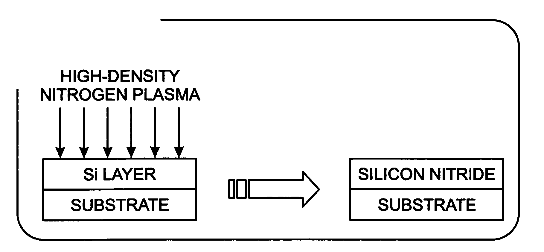
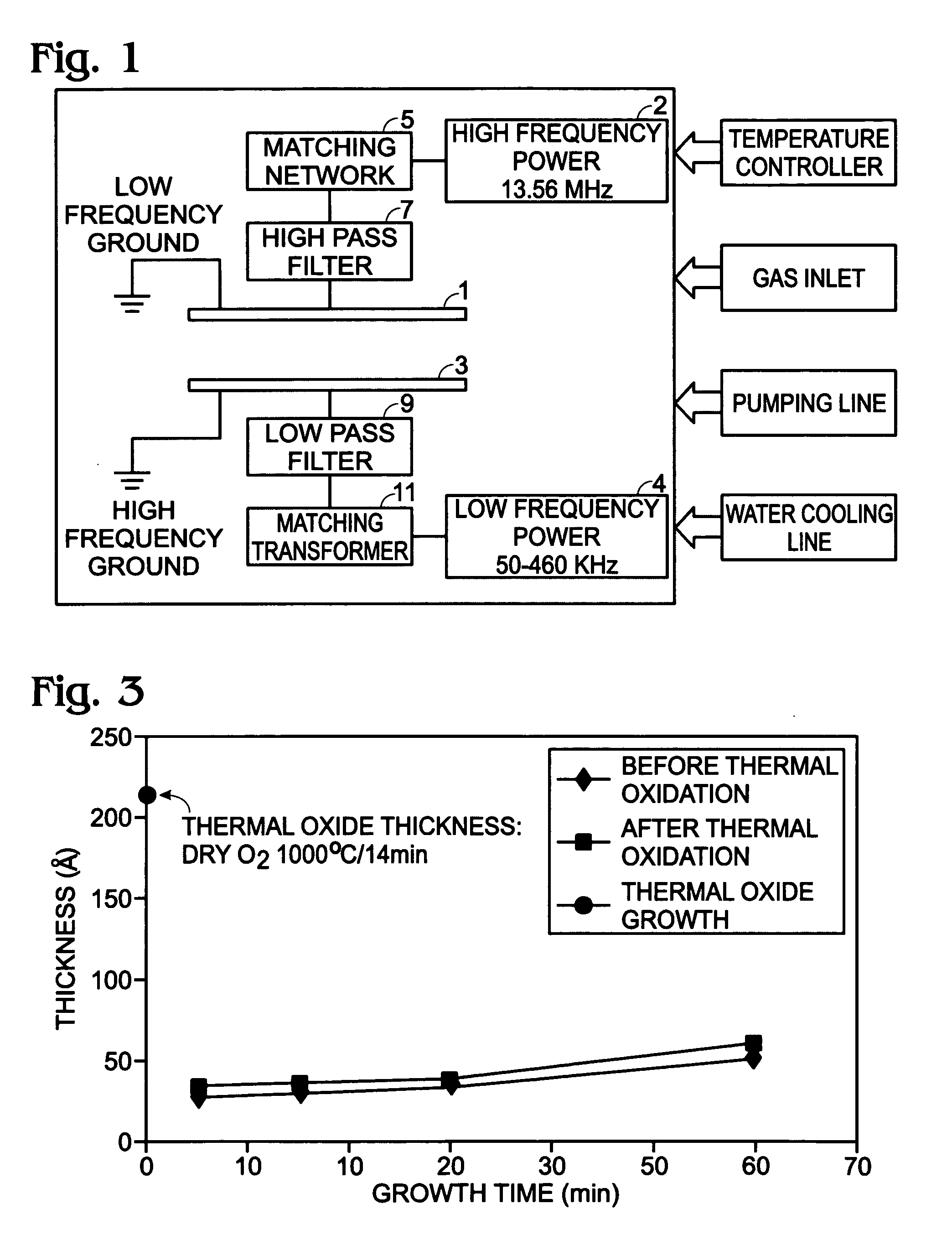
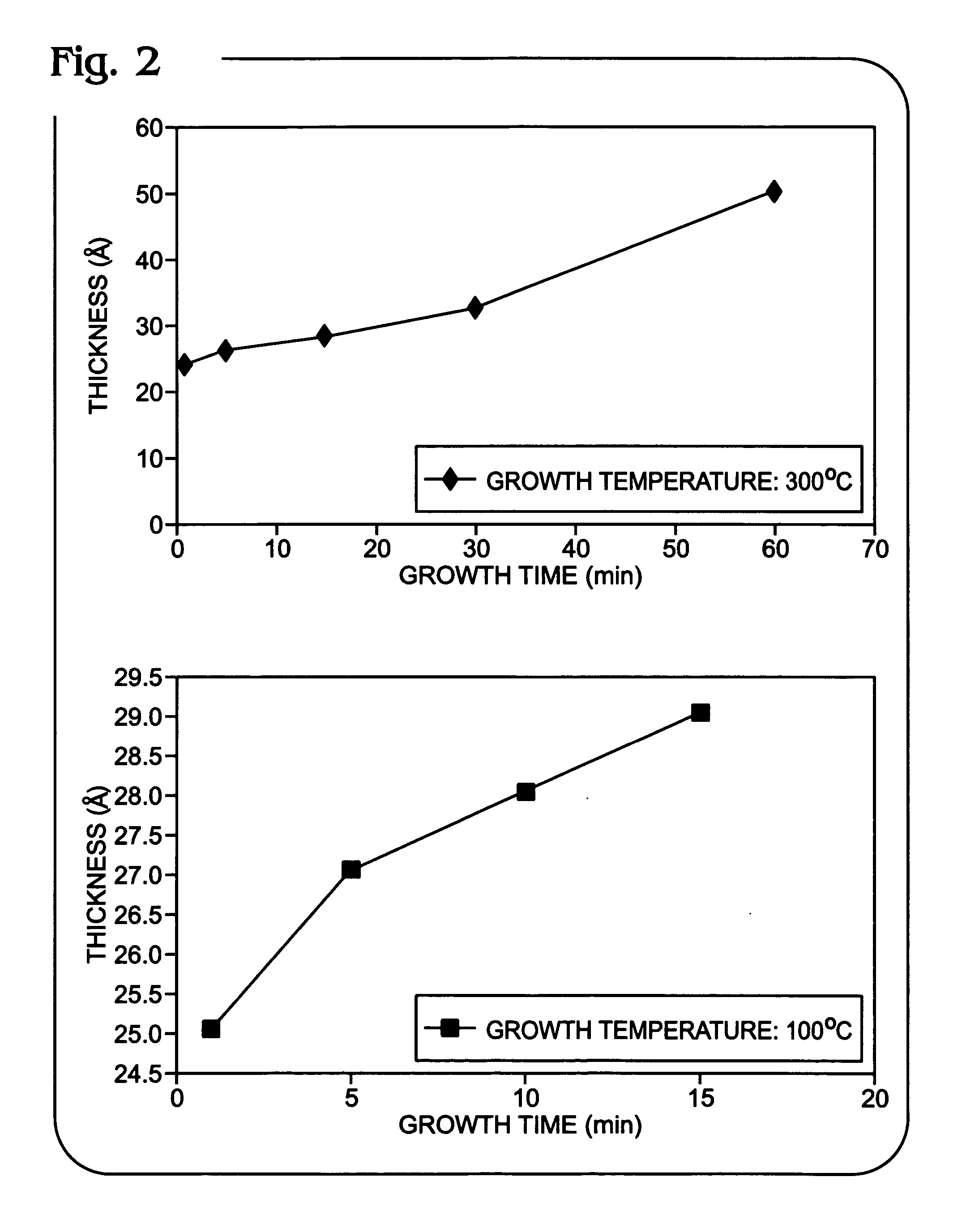
[0026] The present invention provides a high-density plasma based process for the low temperature growth of thermal quality silicon nitride films. The high-density plasma characteristics are effective in the low temperature (

[0027] The HDP nitride growth processes described herein can also be performed at temperatures higher than about 400° C. There are no inherent limitations to the HDP process that prevent the HDP process from being performed at temperatures greater than about 400° C., and as high as thermal process temperatures. However, the ability of the present invention process to g...


PUM

PropertyMeasurementUnit
frequencyaaaaaaaaaa
pressureaaaaaaaaaa
temperaturesaaaaaaaaaa

Abstract

A method is provided for forming a silicon nitride (SiNx) film. The method comprises: providing a Si substrate or Si film layer; optionally maintaining a substrate temperature of about 400 degrees C., or less; performing a high-density (HD) nitrogen plasma process where a top electrode is connected to an inductively coupled HD plasma source; and, forming a grown layer of SiNx overlying the substrate. More specifically, the HD nitrogen plasma process includes using an inductively coupled plasma (ICP) source to supply power to a top electrode, independent of the power and frequency of the power that is supplied to the bottom electrode, in an atmosphere with a nitrogen source gas. The SiNx layer can be grown at an initial growth rate of at least about 20 Å in about the first minute.

Description

RELATED APPLICATIONS [0001] This application is a continuation-in-part of a pending patent application entitled, HIGH-DENSITY PLASMA PROCESS FOR SILICON THIN-FILMS, invented by Pooran Joshi, Ser. No. 10 / 871,939, filed Jun. 17, 2004. [0002] This application is a continuation-in-part of a pending patent application entitled, HIGH-DENSITY PLASMA HYDROGENATION, invented by Joshi et al., Ser. No. 11 / 013,605, filed Dec. 15, 2004. [0003] This application is a continuation-in-part of a pending patent application entitled, METHODS FOR FABRICATING OXIDE THIN-FILMS, invented by Joshi et al., Ser. No. 10 / 801,374, filed Mar. 15, 2004. These applications are incorporated herein by reference.BACKGROUND OF THE INVENTION [0004] 1. Field of the Invention [0005] This invention generally relates to integrated circuit (IC) and liquid crystal display (LCD) fabrication and, more particularly, to high density plasma (HDP) nitration and HDP silicon nitride growth processes. [0006] 2. Description of the Rela...

Claims


Application Information

Patent Timeline
Patent Type & Authority Applications(United States)
IPC IPC(8): H01L21/469H01L21/336H01L21/84H01L29/786
CPCC23C16/24C23C16/45523C23C16/509H01L21/049H01L21/31612H01L29/66666H01L29/6675H01L29/78642H01L21/0217H01L21/02247H01L21/02252H01L21/02329H01L21/0234
Inventor JOSHI, POORAN CHANDRAVOUTSAS, APOSTOLOS T.HARTZELL, JOHN W.
Owner SHARP LAB OF AMERICA INC
Why Eureka
Try Eureka