Surface emitting laser device and production method

a laser device and surface technology, applied in the direction of semiconductor lasers, laser details, electrical devices, etc., can solve the problems of high output of surface emitting lasers, rise of heat generated in laser devices, and difficult to maintain the oscillation in single fundamental transverse mode, so as to facilitate the second resonance region, easy to fabricate a surface emitting laser device, and high output

Inactive Publication Date: 2006-05-04
RICOH KK
View PDF16 Cites 39 Cited by
  • Summary
  • Abstract
  • Description
  • Claims
  • Application Information

AI Technical Summary

Benefits of technology

[0069] According to the other method of producing a surface emitting laser device of the present invention, the second resonance region is formed by steps of forming a semiconductor layer for use of the spacer layer to a predetermined thickness, etching and removing the semiconductor layer on the surface of the surface emitting laser device, and etching and removing the semiconductor layer in the predetermined region, in which the second resonance region is not provided, so as to have a thickness satisfying optical multiple-reflection conditions in the distributed Bragg reflectors. As a result, it is possible to easily form the second resonance region when the second resonance region is provided near the surface of the distributed Bragg reflector. In other words, according to the other method of the present invention, it is possible to easily fabricate a surface emitting laser device capable of operation at high output in the single fundamental transverse mode.
[0070] In addition, because the step of etching and removing the semiconductor layer in the predetermined region is performed by a combination of dry etching and wet etching, it is possible to fabricate the second resonance region with a uniform shape and good reproducibility.
[0071] According to the surface emitting laser module of the present invention, which includes the surface emitting laser device as described above, or the above mentioned surface emitting laser array including plural of the surface emitting laser devices, it is possible to provide a surface emitting laser module capable of oscillation at high output in the fundamental transverse mode and capable of reliable coupling with an optical fiber, and able to suppress the high order mode oscillation. As a result, even when operating conditions (for example, output level) of the module change, the coupling condition and the optical input to the optical fiber barely change. In addition, because of a low resistance, high-speed operations can be realized. In other words, according to the present invention, it is possible to provide a surface emitting laser module of high reliability and capable of high-speed operation at high output in the single fundamental transverse mode.
[0072] According to the electrophotographic system of the present invention, which includes the surface emitting laser device as described above, or the above mentioned surface emitting laser array including plural of the surface emitting laser devices, if the surface emitting laser device or the surface emitting laser array is used as a write light source in the electrophotographic system, because the outgoing laser beam is circular, it is easy to shape the laser beam. In addition, when the surface emitting laser array is used, because of the high position precision between the lasers or laser arrays, multiple laser beams can be easily condensed by the same lens with good reproducibility. Thus, it is possible to provide a high speed electrophotographic system having a simple optical system, low cost and high resolution.
[0073] According to the optical communication system of the present invention, which includes the surface emitting laser device as described above, or the above mentioned surface emitting laser array including plural of the surface emitting laser devices, because the surface emitting laser device and the surface emitting laser array are capable of oscillation at high output in the fundamental transverse mode, it is possible to obtain reliable coupling with an optical fiber. In addition, because the high order mode oscillation is suppressed, the coupling condition and the optical input to the optical fiber barely change even when operating conditions (for example, output level) of the laser device or laser array change. In addition, because of a low resistance, high-speed operations can be realized. Further, because high output is obtainable compared to the related art, it is possible to realize long distance communications. In other words, according to the present invention, it is possible to provide an optical communication system of high reliability and stable coupling with the optical fiber and capable of high speed communications.
[0074] According to the optical interconnection system of the present invention, which includes the surface emitting laser device as described above, or the above mentioned surface emitting laser array including plural of the surface emitting laser devices, because the surface emitting laser device and the surface emitting laser array are capable of oscillation at high output in the fundamental transverse mode, it is possible to obtain reliable coupling with an optical fiber. In addition, because the high order mode oscillation is suppressed, the coupling condition and the optical input to the optical fiber barely change even when operating conditions (for example, output level) of the laser device or laser array change. In addition, because of a low resistance, high-speed operations can be realized. In other words, according to the present invention, it is possible to provide an optical interconnection system of high reliability and stable coupling with the optical fiber and capable of high speed transmission.

Problems solved by technology

On the other hand, because of the small volume of the active layer, it is difficult for the surface emitting laser to obtain high output.
However, it is difficult to maintain the oscillation in the single fundamental transverse mode even at high output.
Further, heat generated in the laser device rises due to an increased resistance; as a result, it becomes difficult to obtain high output.
When actually driving the laser device, it is known that it is difficult to maintain the oscillation in the single fundamental transverse mode in a current highly-injected region because of the refractive index changes caused by heat generation in a current passage and plasma effect of injected carrier, gain saturation of the single fundamental transverse mode due to a spatial hole burning effect.
However, as is known, this kind device suffers from oscillation delay, or poor stability of the transverse mode.
As described above, it is difficult to obtain stable oscillation in the single fundamental transverse mode at high output with either the selective oxidation surface emitting laser device or the hydrogen ion implantation surface emitting laser device.
However, because the distributed Bragg reflector utilizes multiple-reflections on interfaces of multiple layers, the light intensity is attenuated gradually towards the surface layer; thus, by arranging a reflectivity adjusting structure on the surface of the laser device, it is difficult to add a large mirror loss.
For this reason, in the related art, it is difficult to selectively add a sufficiently large mirror loss, and when the current is injected strongly, oscillation in the high order transverse modes is started.
In other words, the high order transverse mode oscillation cannot be sufficiently suppressed.

Method used


Image

  • Surface emitting laser device and production method
  • Surface emitting laser device and production method
  • Surface emitting laser device and production method

Examples


first embodiment

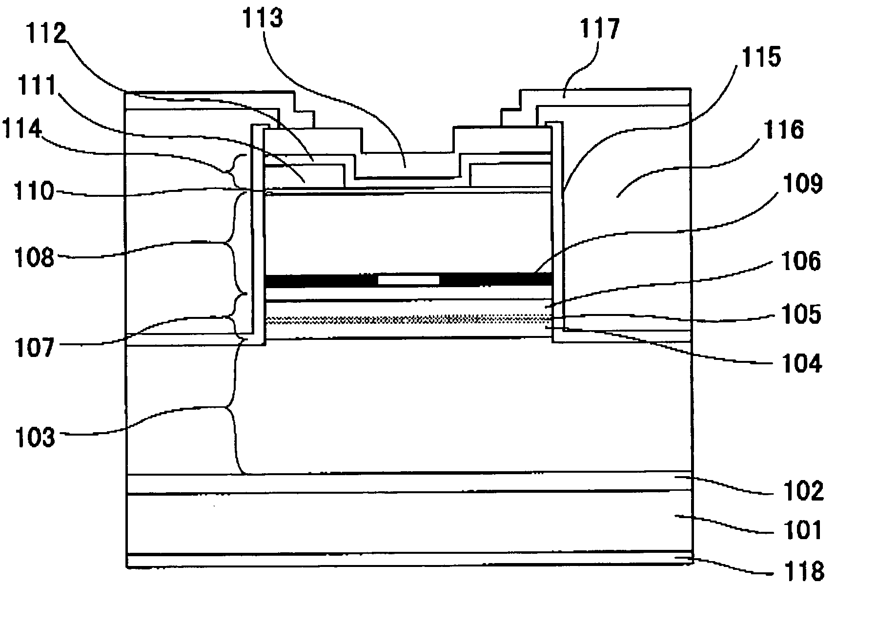
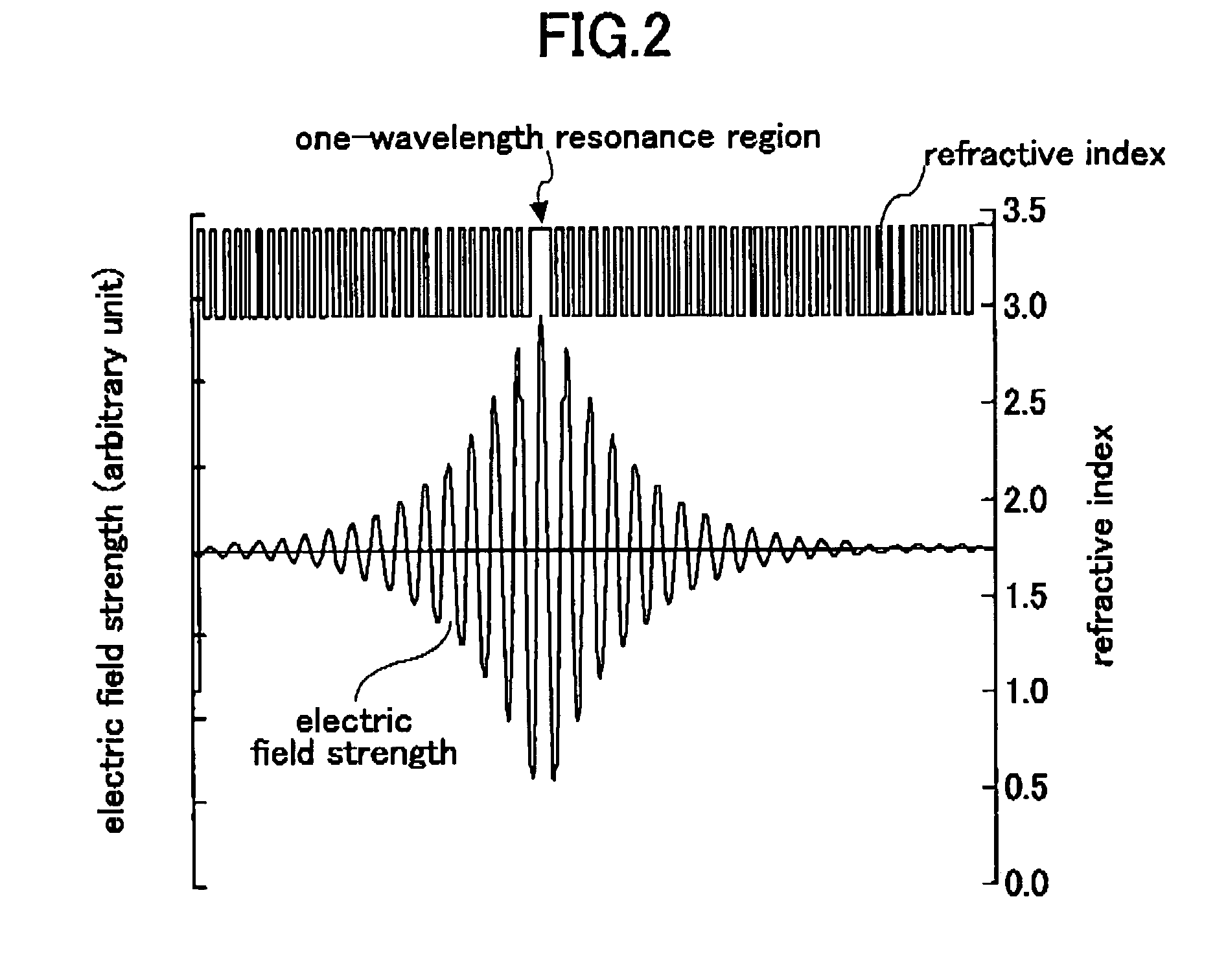
[0098] The present embodiment discloses a surface emitting laser device which includes a first resonance region that has an active layer and spacer layers on two sides of the active layer, two distributed Bragg reflectors that sandwich the resonance region and face each other with each of the distributed Bragg reflectors having periodically stacked low refractive index layers and high refractive index layers, and a current confinement structure that defines a current injection region for injecting a current into the active layer. In the surface emitting laser device, at least one of the distributed Bragg reflectors includes a second resonance region, which is arranged in the current injection region excluding a predetermined region surrounding the center of the current injection region. For example, the center is that of a cross-section of the current injection region parallel to the substrate, for example, when the cross-section of the current injection region is a circle, a four-s...

second embodiment

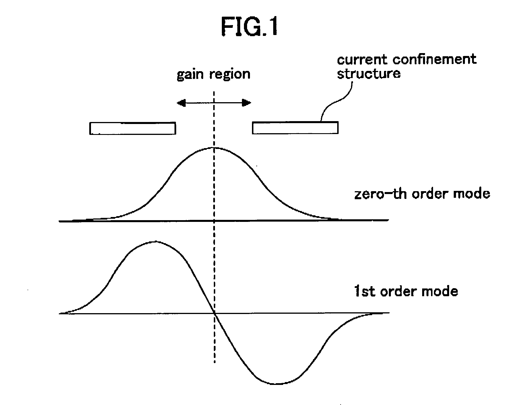
[0125] The present embodiment discloses a surface emitting laser device which has a structure similar to that in the first embodiment. In addition, in the surface emitting laser device of the present embodiment, at least part of the range within a distance from the center of the current injection region is within a boundary of the current injection region, and the second resonance region partially spatially overlaps with the current injection region.

[0126] In the surface emitting laser device of the present embodiment, as described previously, because the second resonance region is provided in an area at the middle of the distributed Bragg reflector corresponding to the high order transverse modes, and because of the resonance action in the second resonance region, it is possible to highly efficiently increase the mirror loss for the high order transverse mode oscillation, and as a result, it is possible to efficiently suppress the high order transverse mode oscillation. Therefore,...

third embodiment

[0138] The present embodiment discloses a surface emitting laser device which has a structure similar to that in the first embodiment. In addition, in the surface emitting laser device of the present embodiment, the region without the second resonance region extends out of a boundary of the current injection region, which is defined by the current confinement structure.

[0139] In the surface emitting laser device of the present embodiment, as described previously, because the second resonance region is provided in an area at the middle of the distributed Bragg reflector corresponding to the high order transverse modes, and because of the resonance action in the second resonance region, it is possible to highly efficiently increase the mirror loss for the high order transverse mode oscillation, and thus to efficiently suppress the high order transverse mode oscillation.

[0140] Because the width of the fundamental transverse mode distribution approximately corresponds to the size of t...


PUM


Abstract

A surface emitting laser device is disclosed that is able to selectively add a sufficiently large loss to a high order transverse mode so as to efficiently suppress a high order transverse mode oscillation and to oscillate at high output in a single fundamental transverse mode. The surface emitting laser device includes a first resonance region that includes an active layer and spacer layers, two distributed Bragg reflectors that sandwich the resonance region, and a current confinement structure that defines a current injection region for the active layer. At least one of the distributed Bragg reflectors includes a second resonance region arranged in the current injection region excluding a predetermined region surrounding a center of the current injection region.

Description

BACKGROUND OF THE INVENTION [0001] 1. Field of the Invention [0002] The present invention relates to a surface emitting laser device, a surface emitting laser array, a method of producing the surface emitting laser device, a surface emitting laser module, an electrophotographic system, an optical communication system, and an optical interconnection system. [0003] 2. Description of the Related Art [0004] Because a surface emitting laser (for example, a surface emitting semiconductor laser) has a small-volume active layer and is capable of operations at a low threshold current and high speed modulation compared to an edge-emitting laser, it is attracting attention as a light source in a LAN (Local Area Network) or the like. In addition, since the surface emitting laser emits a laser beam in a direction perpendicular to a substrate thereof, it is easy to construct a two-dimensional array structure; thus, it is expected that the surface emitting laser is to be used as a light source for...

Claims


Application Information

Patent Timeline
Patent Type & Authority Applications(United States)
IPC IPC(8): H01S5/00
CPCH01S5/18313H01S5/18327H01S5/18358H01S5/423H01S2301/166H01S5/02345
Inventor JIKUTANI, NAOTO
Owner RICOH KK
Why Eureka
Try Eureka