Semiconductor packages with asymmetric connection configurations

a technology of asymmetric connection and semiconductor chip, which is applied in the field of lead frame, can solve the problems of electromagnetic and/or electrostatic coupling between signal lines, interference with the proper functioning of the device, and the increase in the processing speed of the active regions formed on the semiconductor chip, so as to improve the performance and stability of the resulting devi

Inactive Publication Date: 2006-05-18
SAMSUNG ELECTRONICS CO LTD
View PDF11 Cites 6 Cited by
  • Summary
  • Abstract
  • Description
  • Claims
  • Application Information

AI Technical Summary

Benefits of technology

[0021] As provided in more detail below, the invention allows for the independent adjustment of the electrical properties of the fixed voltage lines

Problems solved by technology

Within the semiconductor industry, there is a realization that merely increasing the processing speed of the active regions formed on a semiconductor chip will not necessarily translate into system processing improvements.
As the size of the various connection components decreases and/or the speed of the associated semiconductor device increases with any conductive line carrying a signal the electromagnetic and electrostatic fields generated by the various conductors can interfere with the proper functioning of the device.
As will be appreciated, electromagnetic and/or electrostatic coupling between signal lines, also referred to as “cross-talk,” is undesirable because it increases the load of the signal lines and may create noise and/or signal delays.
Even when the active signal line is sufficiently isolated

Method used


Image

  • Semiconductor packages with asymmetric connection configurations
  • Semiconductor packages with asymmetric connection configurations
  • Semiconductor packages with asymmetric connection configurations

Examples


first embodiment

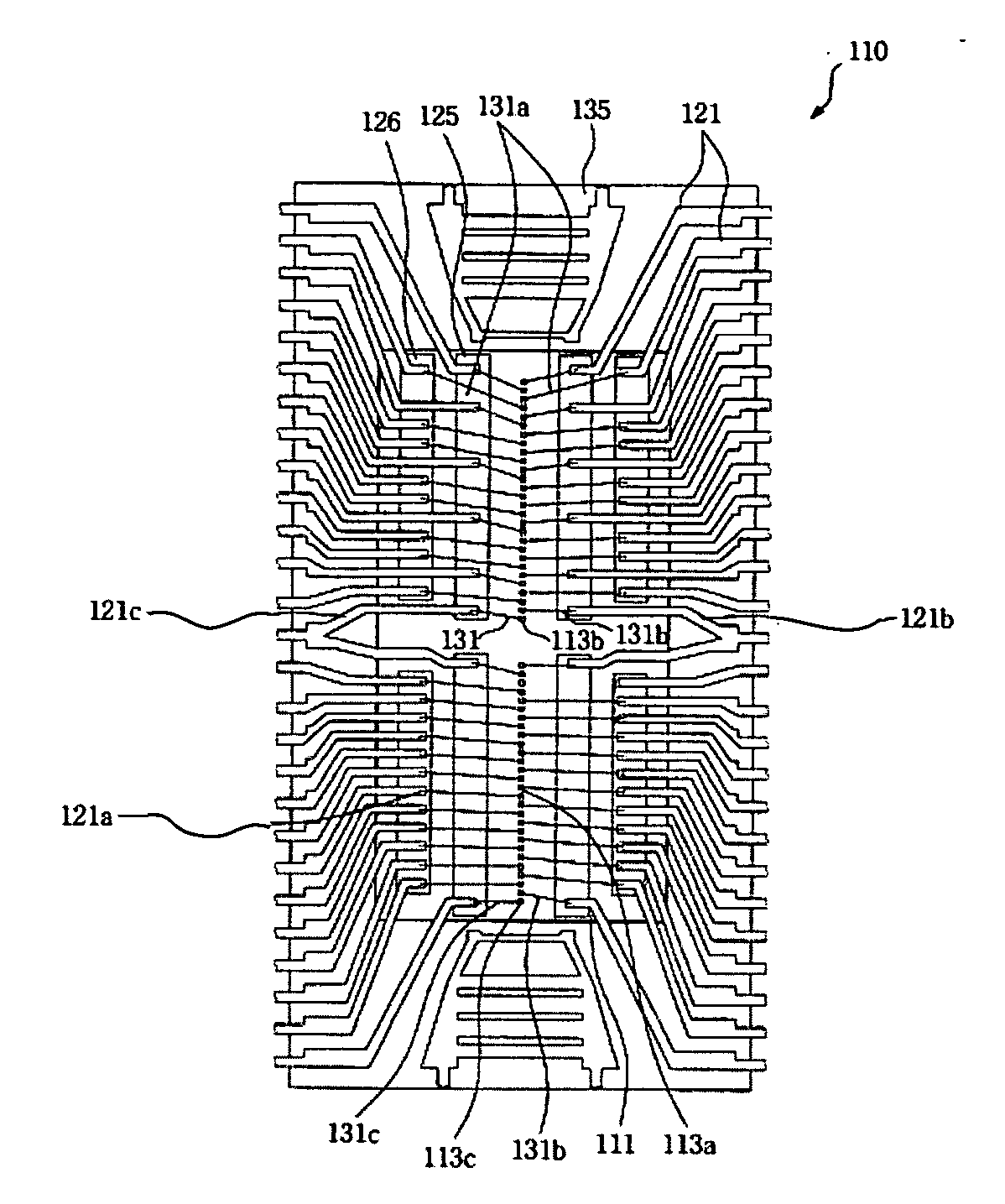
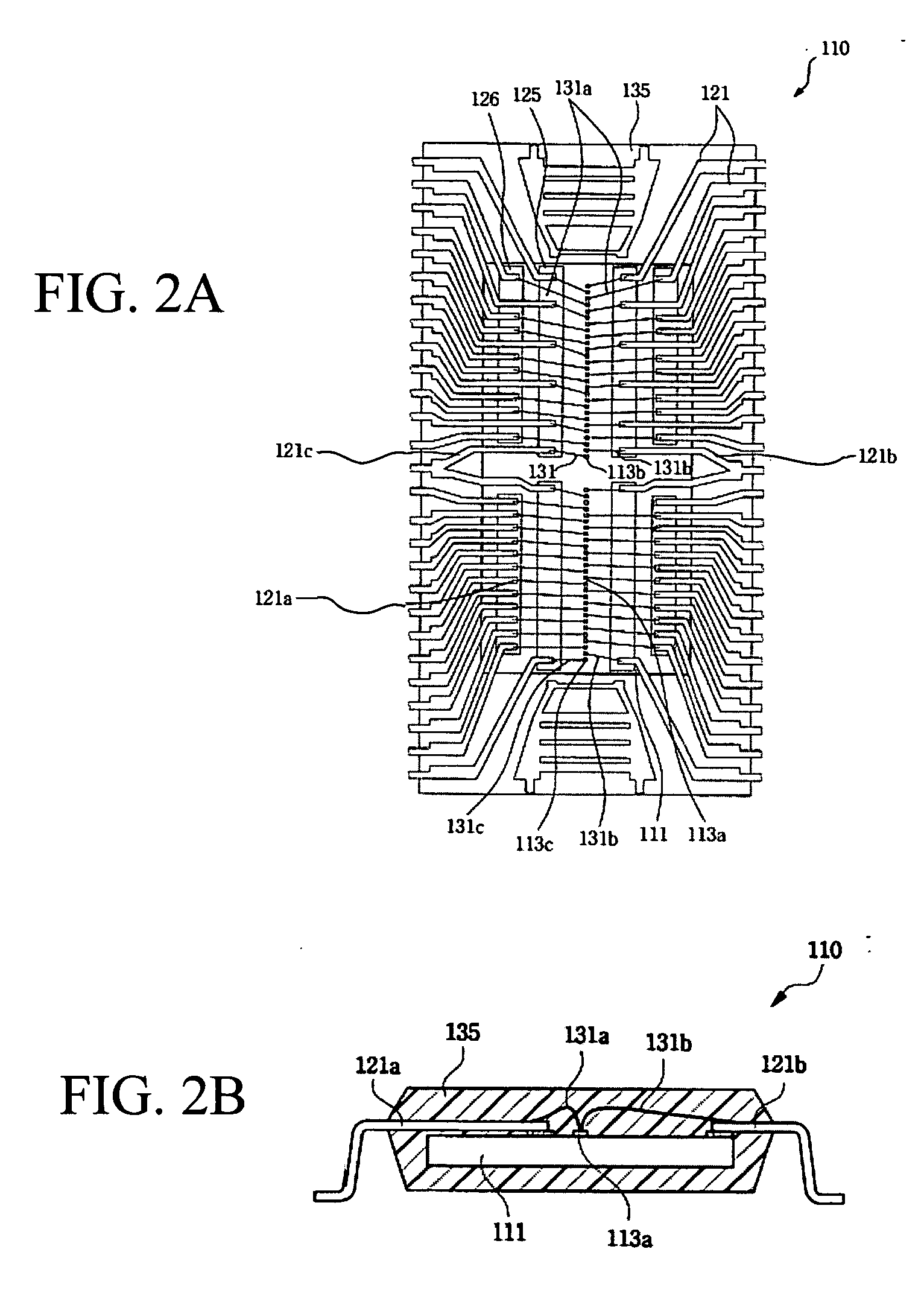
[0034]FIGS. 2A and 2B illustrate a plan view and a cross-sectional view respectively of a semiconductor device having a LOC configuration in accord with an example embodiment of the invention. As illustrated in FIG. 2A, the semiconductor device includes a semiconductor chip 111 having an active surface, for example a DRAM device, having a center-pad configuration. The semiconductor chip is attached on a bottom surface of leads 121 by adhesive tapes 125, 126. Chip pads 113 are connected to the leads by bonding wires 131. The semiconductor chip, the leads and the bonding wires are encapsulated within a molding compound 135.

[0035] As illustrated in FIG. 2A, particularly in comparison with the device illustrated in FIG. 1A, the semiconductor device having a LOC configuration in accord with an example embodiment of the invention includes two different connector configurations. The first configuration is utilized to form electrical connections to the various signal bonding pads 113a and ...

second embodiment

[0037]FIG. 3A illustrates a plan view and of a semiconductor device having a LOC configuration in accord with another example embodiment of the invention. As illustrated in FIG. 3A, the semiconductor device includes a semiconductor chip 411 having an active surface, for example a DRAM device, having three separate rows of bonding pads, including a first plurality of bonding pads 413b, 413c arranged in a center-pad configuration and a second plurality of bonding pads 413a arranged in two additional rows positioned between the center-pad row and opposite edges of the semiconductor chip.

[0038] The semiconductor device also includes a first plurality of leads 421a that extend a first average length LS over the active surface of the semiconductor chip 411 and a second plurality of leads 421b, 421c that extend a second average length LPG over the active surface, where LSPG. The various pluralities of leads 421a-c can be attached to the active surface of the semiconductor with one or more...

third embodiment

[0039] As illustrated in FIGS. 4A and 4B, another example embodiment of the invention can be utilized in manufacturing an improved QFP (Quad Flat Package) using an asymmetric configuration similar to that detailed above in connection with the first example embodiment. As illustrated in FIG. 4A, although none of the leads extend over the active surface of the semiconductor chip 211, those leads associated with the fixed voltage lines 221b, 221c extend closer to the edge of the semiconductor chip while those associated with the signal lines 221a a terminated further from the edge of the semiconductor chip. Also, in addition to the variations in length, those leads corresponding to fixed voltage lines may be relatively wider than those corresponding to signal lines, thereby further increasing the average difference in capacitance and further stabilizing the fixed voltage lines.

[0040] Accordingly, the bonding wires 231b, 231c that connect the fixed voltage leads to the corresponding pe...


PUM


Abstract

Provided are semiconductor devices and methods for configuring lead frames and/or device bonding pads to provide for the independent adjustment of the electrical characteristics of both fixed voltage lines, e.g., Vdd and Vss, and the signal lines, e.g., command, clock, data and address. In particular, the invention provides for adjusting the relative sizing of leads corresponding to fixed voltage lines and signal lines for increasing the relative capacitance on the fixed voltage lines to improve their stability will reducing the noise on the signal lines. The invention may be utilized with a variety of package configurations including lead-on-chip LOC configurations, more conventional quad flat pack QFP configurations in which the leads do not extend past the perimeter of the semiconductor chip or hybrid configurations in which some leads do extend past the perimeter of the semiconductor chip and across the active surface.

Description

PRIORITY STATEMENT [0001] This U.S. non-provisional application claims benefit of priority under 35 U.S.C. § 119 from Korean Patent Application No. 2004-0092447, filed on Nov. 12, 2004, the entire contents of which are incorporated herein by reference. BACKGROUND OF THE INVENTION [0002] 1. Field of the Invention [0003] The invention relates to lead frames used for connecting electrical signals to packaged integrated circuits including those lead frames configured to extend over an active surface of the integrated circuits, also known as a lead on chip or LOC configuration. By modifying the relative configurations of the fixed voltage leads, e.g., ground and power, and the associated signal leads, lead frames according to the invention generally reduce connection capacitance and the likelihood of coupling between adjacent signal lines and improve the stability of the fixed voltage leads. [0004] 2. Description of the Related Art [0005] Conventional LOC packaging techniques for high-sp...

Claims


Application Information

Patent Timeline
IPC IPC(8): H01L23/52
CPCH01L23/4951H01L24/05H01L24/06H01L2224/04042H01L2224/05556H01L2224/05599H01L2224/06136H01L2224/48091H01L2224/48247H01L2224/4826H01L2224/48463H01L2224/49171H01L2224/49433H01L2224/73215H01L2224/73265H01L2224/85399H01L2924/01082H01L2924/014H01L2924/19041H01L2924/3011H01L2924/00014H01L24/48H01L24/49H01L2224/32245H01L2924/01005H01L2924/01006H01L2924/01033H01L2924/01055H01L2224/45099H01L2924/00H01L2924/30107H01L2224/05554H01L2924/14H01L2924/181H01L2924/00012H01L21/60
Inventor AHN, MEE-HYUNLEE, JONG-JOOLEE, YONG-JAE
Owner SAMSUNG ELECTRONICS CO LTD
Why Eureka
Try Eureka