Field effect transistor and method of manufacturing the same

a field effect transistor and field effect technology, applied in the field of field effect transistors, can solve the problems of high output, rapid increase in electric current, and storage of holes produced, and achieve the effect of high outpu

Active Publication Date: 2006-05-25
NICHIA CORP
View PDF28 Cites 98 Cited by
  • Summary
  • Abstract
  • Description
  • Claims
  • Application Information

AI Technical Summary

Benefits of technology

[0011] To attain the above object, a field effect transistor according to a first aspect of the present invention comprises an i-type first semiconductor layer and a second semiconductor layer formed on the first semiconductor layer and having a band gap energy greater than that of the first semiconductor layer. In this field effect transistor, the first semiconductor layer and second semiconductor layer are each made of a gallium nitride-based compound semiconductor layer, a gate electrode is formed on the second semiconductor layer, a second electrode is formed on the first semiconductor layer, and the first semiconductor layer and second semiconductor layer are interposed between the gate electrode and the second electrode. By using this construction, the holes stored in the channel become able to be discharged from the relevant element, so that it is possible to enhance the withstand voltage of the field effect transistor.
[0033] According to a field effect transistor and a method of manufacturing it according to the present invention, the holes that have occurred from the first semiconductor layer can be discharged from the second electrode with a high efficiency. Accordingly, the field effect transistor can be made the one that avoids the breakdown of the device due to the storage of the hole and that can have higher withstand voltage and can provide, i.e., comply with, a high output.

Problems solved by technology

The problem regarding the collision ionization is that the holes that have been produced are stored in the electron transit layer.
As a result of this, collision ionization is promoted, with the result that a larger number of holes are stored to cause a rapid increase in the electric current.
This goes beyond the limit of the withstand voltage of the device to cause breakdown of it.
However, to realize this construction, there exist very difficult problems to solve.
However, it is not easy to make hydrogen removal, in a structure wherein on the Mg doped GaN layer grown on a sapphire substrate there are further laminated layers, to such art extent, by annealing treatment, as the Mg-doped GaN layer which is located under exhibits a p-type one.
In addition, since forming the p-type GaN layer results in forming a large capacitance over an entire surface of p-type layer, there is also the problem that it becomes difficult to make the device operation higher in speed.
Further, since, regarding the p-type layer, there is the need to dope a large amount of impurity, the crystallinity of the p-type layer tends to be very bad.
This is a problem that is peculiar to a gallium nitride-based compound semiconductor.
Accordingly, when providing a p-type layer on the substrate side of the channel, the crystallinity per se of respective layers formed on the p-type layer whose crystallinity is inferior becomes deteriorated, with the result that the tendency that the characteristics as those of the device get deteriorated occurs.
Also, when applying a voltage to the HEMT of the electrode structure such as that illustrated in FIG. 1, an electric field which is higher than the electric field applied in the other part is inconveniently applied at the drain terminal of the gate electrode.

Method used


Image

  • Field effect transistor and method of manufacturing the same
  • Field effect transistor and method of manufacturing the same
  • Field effect transistor and method of manufacturing the same

Examples


Embodiment Construction

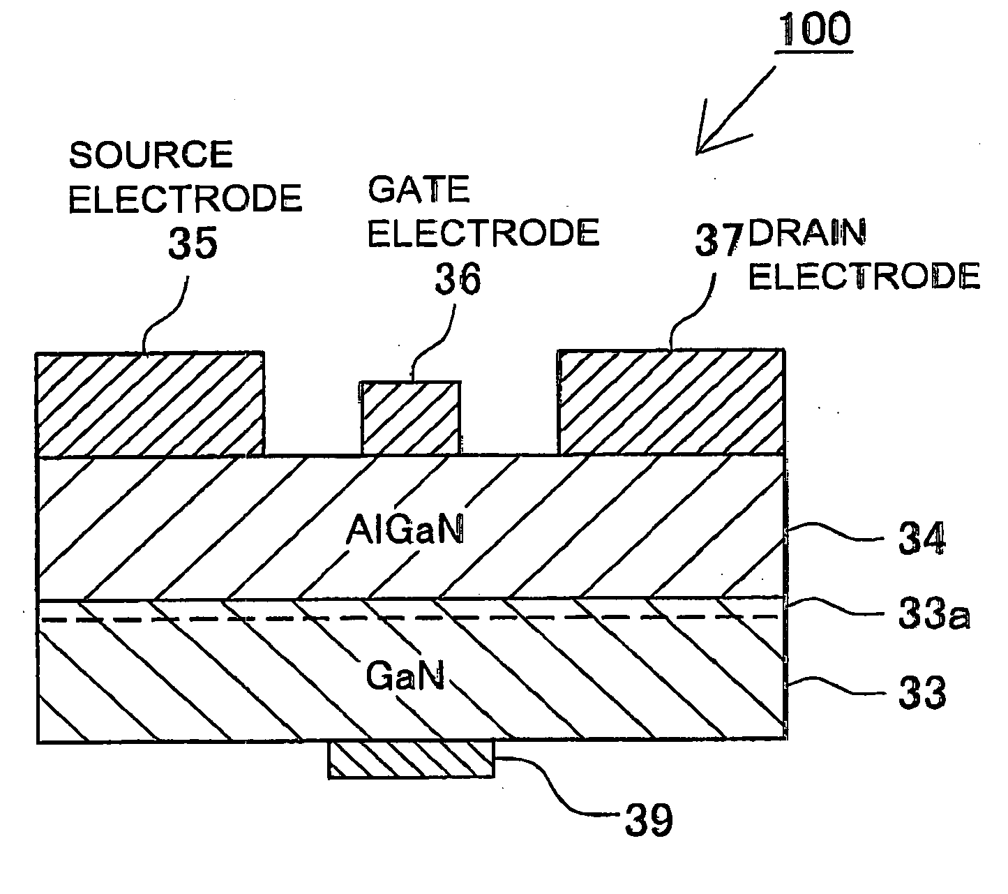
[0046]FIG. 3 illustrates an example constructing a GaN-based HEMT 100, as the field effect transistor according to an embodiment of the present invention. The HEMT 100 illustrated in this figure has a construction in which a carrier transit layer 33 as a first semiconductor layer and a carrier supply layer 34 as a second semiconductor layer are sequentially laminated. On an upper surface of the carrier supply layer 34, there are formed a source electrode 35, gate electrode 36, and drain electrode 37. In this embodiment, a monopolar device that uses electrons as the carriers will be explained. However, in a case where using holes prepared by making the conductivity type of the carriers opposite, the device can be made a transistor using the holes. Namely, in such a device, the carriers of a conductivity opposite to that of the carriers, i.e., electrons are discharged via the second electrode. In this structure of GaN-based HEMT 100, the carrier supply layer 34 supplies electrons to t...


PUM


Abstract

A field effect transistor includes an i-type first semiconductor layer and a second semiconductor layer that is formed on the first semiconductor layer and the band gap energy of that is higher in magnitude than that of the first semiconductor layer. The first semiconductor layer and second semiconductor layer are each made of a gallium nitride-based compound semiconductor layer. A gate electrode 36 is formed on the second semiconductor layer; and a second electrode 39 is formed on the first semiconductor layer. Thus, the field effect transistor is constructed in such a manner as the first semiconductor layer and second semiconductor layer are interposed between the gate electrode 36 and the second electrode 39. By constructing like this, it is possible to discharge the holes that are accumulated in the channel from the elemental structure and to improve the withstand voltage of the field effect transistor.

Description

BACKGROUND OF THE INVENTION [0001] 1. Field of the Invention [0002] The present invention relates to a field effect transistor that uses gallium nitride-based compound semiconductor. [0003] 2. Description of the Related Art [0004] Since a gallium nitride-based compound semiconductor is wide in forbidden band, a field effect transistor (FET) using that semiconductor is capable of being operated at a high frequency and in addition at a high withstand voltage. So, It is expected as a high-output power semiconductor device. And there have up to now been proposed a metal semiconductor FET (MESFET), a high electron mobility transistor (HEMT), and so on. The HEMT is a high-speed semiconductor device which has become popular as the devices operating at a high frequency. Specifically, regarding this, a device that uses a GaAs / AlGaAs heterojunction has been put to practical use. Because of its excellent microwave / millimeter wave characteristics, that device has widely been used as a low-noise...

Claims


Application Information

Patent Timeline
Patent Type & Authority Applications(United States)
IPC IPC(8): H01L31/0328H01L29/80H01L29/739H01L21/338H01L29/778H01L29/812
CPCH01L21/6835H01L29/2003H01L29/402H01L29/42316H01L29/66462H01L29/7787H01L2221/6835H01L2924/30105H01L29/1075
Inventor TANIMOTO, MASASHI
Owner NICHIA CORP
Why Eureka
Try Eureka