Strained silicon fin structure

a technology of strained silicon fins and strained channels, which is applied in the direction of semiconductor devices, electrical equipment, transistors, etc., can solve the problems of reducing the threshold voltage and the increase of sub-threshold current, reducing the ability of the gate to control the operation of the device, and the scaling of conventional bulk mosfet devices beyond the 50 nm process generation is very difficult, so as to reduce the short channel effect, enhance drive current, and enhance carrier mobility

Inactive Publication Date: 2006-06-01
MICROSOFT TECH LICENSING LLC +1
View PDF8 Cites 248 Cited by
  • Summary
  • Abstract
  • Description
  • Claims
  • Application Information

AI Technical Summary

Benefits of technology

[0014] The present invention strained silicon channel fin structure can be employed to fabricate a strained silicon finFET device. The present invention strained silicon finFET device comprises a thin strained silicon-containing fin channel standing on an insulator layer, sandwiching between a source and a drain. A gate dielectric and double gates cover the sides of the fin to form the inversion layers on the sides of the channel. The channel fin is sufficiently thin so that the two gates control the entire channel film. The double gates on the channel fin can suppress the short channel effect and enhance drive current. The strained channel can provide enhanced carrier mobility to further improve the device performance. The present invention strained channel finFET device thus can improve hole carrier mobility and / or electron carrier mobility, in addition to suppressing short channel effect.

Problems solved by technology

As the channel length becomes smaller than 100 nm, MOSFET devices experience certain deleterious performance due to their size, such as the short channel effect caused by the close proximity of the source and drain, resulting in the reduction of the threshold voltage and the increase of sub-threshold current.
Thus the interaction between the source and drain of the MOSFET degrades the ability of the gate to control the operation of the device.
Therefore, scaling of conventional bulk MOSFET devices beyond the 50 nm process generations is very difficult.
For example, ultra thin gate oxide (less than 1-2 nm) has significant problem of tunneling current, and ultra shallow junction has significant problem of low sheet resistance and junction lateral steepness.
The thin surface silicon layer limits the volume of silicon that needs to be charged to switch the transistor on and off, and therefore reduces the parasitic capacitance of the transistor and increases the switching speed.

Method used


Image

  • Strained silicon fin structure
  • Strained silicon fin structure
  • Strained silicon fin structure

Examples


Embodiment Construction

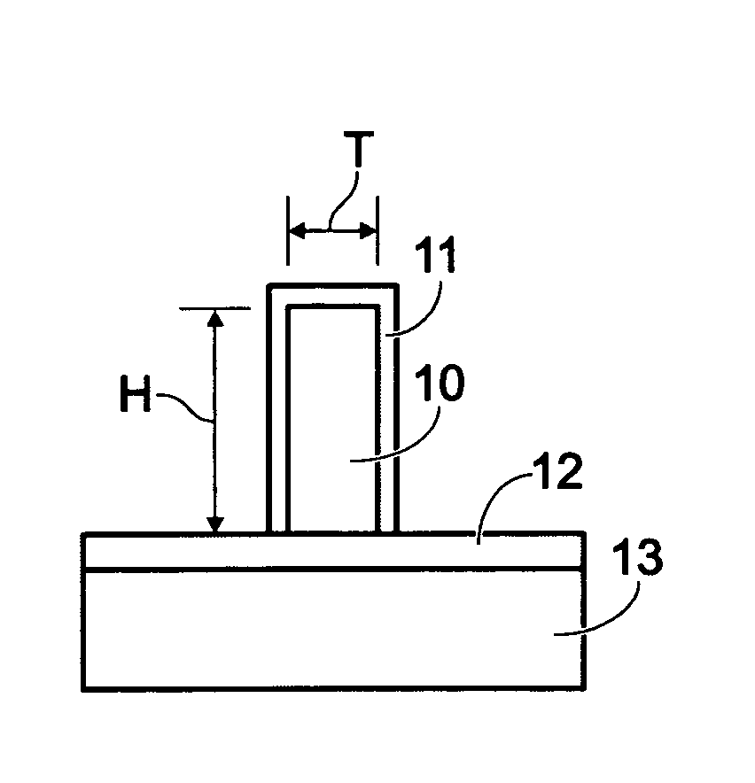
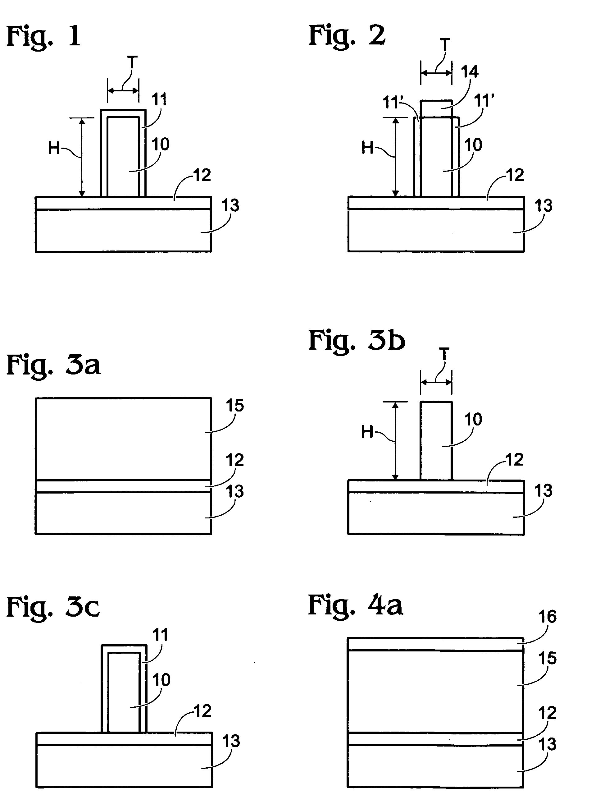
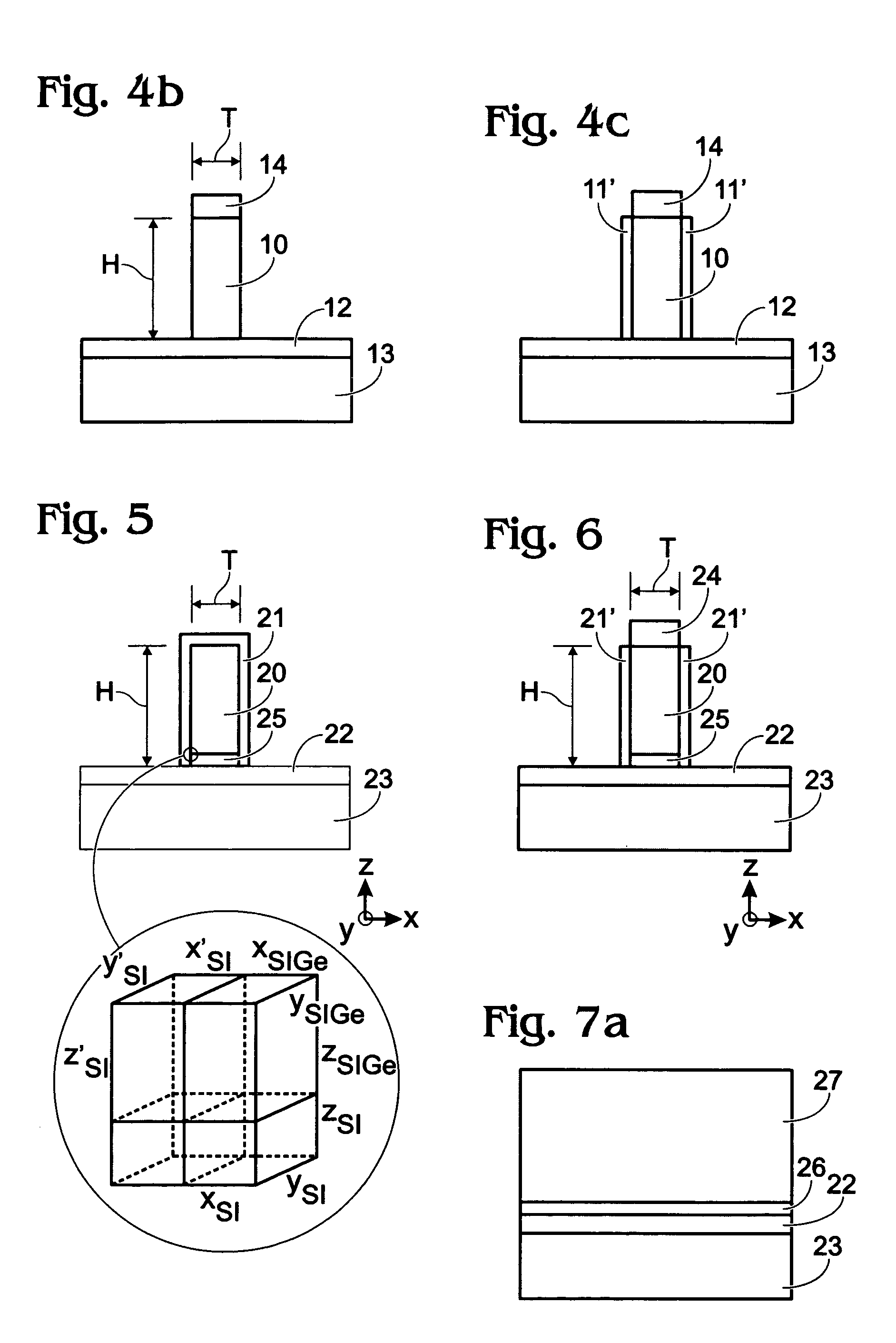
[0033] The present invention discloses a strained silicon fin structure and a strained silicon finFET device employing the disclosed strained silicon fin structure. The strained silicon fin structure is fabricated by forming a silicon-containing epitaxial layer on a silicon-containing seed fin having different lattice constant. The strained silicon finFET device comprises a strained silicon fin structure standing on an insulator layer, sandwiching between a source and a drain with a gate dielectric and a double gates covering the sides of the strained silicon fin structure to form the inversion layers on the sides of the fin.

[0034] The present invention strained silicon fin structure comprises a seed fin structure disposed on an insulator substrate, and a strained channel layer fabricated on the seed fin structure. The channel layer material has a lattice constant different than the lattice constant of the seed fin material, and therefore the channel layer becomes a strained channe...


PUM


Abstract

Disclosing is a strained silicon finFET device having a strained silicon fin channel in a double gate finFET structure. The disclosed finFET device is a double gate MOSFET consisting of a silicon fin channel controlled by a self-aligned double gate for suppressing short channel effect and enhancing drive current. The silicon fin channel of the disclosed finFET device is a strained silicon fin channel, comprising a strained silicon layer deposited on a seed fin having different lattice constant, for example, a silicon layer deposited on a silicon germanium seed fin, or a carbon doped silicon layer deposited on a silicon seed fin. The lattice mismatch between the silicon layer and the seed fin generates the strained silicon fin channel in the disclosed finFET device to improve hole and electron mobility enhancement, in addition to short channel effect reduction characteristic inherently in a finFET device.

Description

RELATED APPLICATIONS [0001] This application is a Divisional of a pending patent application entitled, Strained silicon finFET device, invented by Lee et al., Ser. No. 10 / 602,436, filed Jun. 23, 2003, which is incorporated herein by reference.FIELD OF THE INVENTION [0002] This invention related generally to semiconductor devices including field effect transistors (FETs), metal-oxide-semiconductor FETs (MOSFETs), and more particularly related to improved semiconductor devices having double gates and strained channel. BACKGROUND OF THE INVENTION [0003] Field effect transistors (FET's) and particularly Metal-Oxide-Semiconductor field effect transistors (MOSFETs) are the dominant electronic devices in use today. The performance of these devices has been improved steadily through the reduction in device dimensions, from 10-20 μm channel length in the '70 to 100 nm channel length in '00 technology. [0004] As the channel length becomes smaller than 100 nm, MOSFET devices experience certain...

Claims


Application Information

Patent Timeline
Patent Type & Authority Applications(United States)
IPC IPC(8): H01L29/06H01L21/336H01L29/10H01L29/78H01L29/786
CPCH01L29/1054H01L29/66795H01L29/785H01L29/78687
Inventor LEE, JONG-JANHSU, SHENG TENGTWEET, DOUGLAS J.MAA, JER-SHEN
Owner MICROSOFT TECH LICENSING LLC
Why Eureka
Try Eureka