Integrated semiconductor device and method of manufacturing the same

a semiconductor and integrated technology, applied in semiconductor devices, capacitors, electrical equipment, etc., can solve the problems of low reliability, defect risk of dielectric large changes in dielectric constant of materials having a high dielectric constant, so as to improve reliability, reduce the number of defects, and reduce the density of defects

Inactive Publication Date: 2006-06-15
HITACHI LTD
View PDF4 Cites 12 Cited by
  • Summary
  • Abstract
  • Description
  • Claims
  • Application Information

AI Technical Summary

Benefits of technology

[0009] To solve the above problems, niobium oxide and aluminum oxide layers are laminated together as the dielectric film of a capacitor in the present invention. Particularly, the density of defects is reduced by crystallizing niobium oxide. To reduce the temperature coefficient in particular, the optimal value of the thickness ratio of the aluminum oxide film to the niobium oxide film is used.
[0010] The first effect of the present invention is that the number of defects is reduced by crystallizing niobium oxide to improve reliability. The dielectric loss of niobium oxide which is closely related with defects is generally several % or more when niobium oxide is amorphous and can be reduced to less than 1% when niobium oxide is crystallized. As an effect incidental to the above effect, the dielectric constant of niobium oxide is increased from about 20 in an amorphous state to about 50 by crystallization, thereby improving the density of capacitance. In the case of tantalum oxide of the prior art, since a temperature required for crystallization is about 700° C., tantalum oxide could not be crystallized at a temperature within the heat resistance temperature r...

Problems solved by technology

The first problem to be solved is that a dielectric material having a high dielectric constant is liable to become defective and inferior in reliability as a capacitor.
The second problem is that a material having a high dielectric constant has great changes in dielectric constant caused by temperature variations, whereby its capacitance is changed by variations in ambient temperature and operation conditions with the result of fluctuations in circuit operation.
Further, the third problem is that the above two problems conflict with each other.
That is, when the number of defects is reduced to improve reliability, temperat...

Method used


Image

  • Integrated semiconductor device and method of manufacturing the same
  • Integrated semiconductor device and method of manufacturing the same
  • Integrated semiconductor device and method of manufacturing the same

Examples


embodiment 1

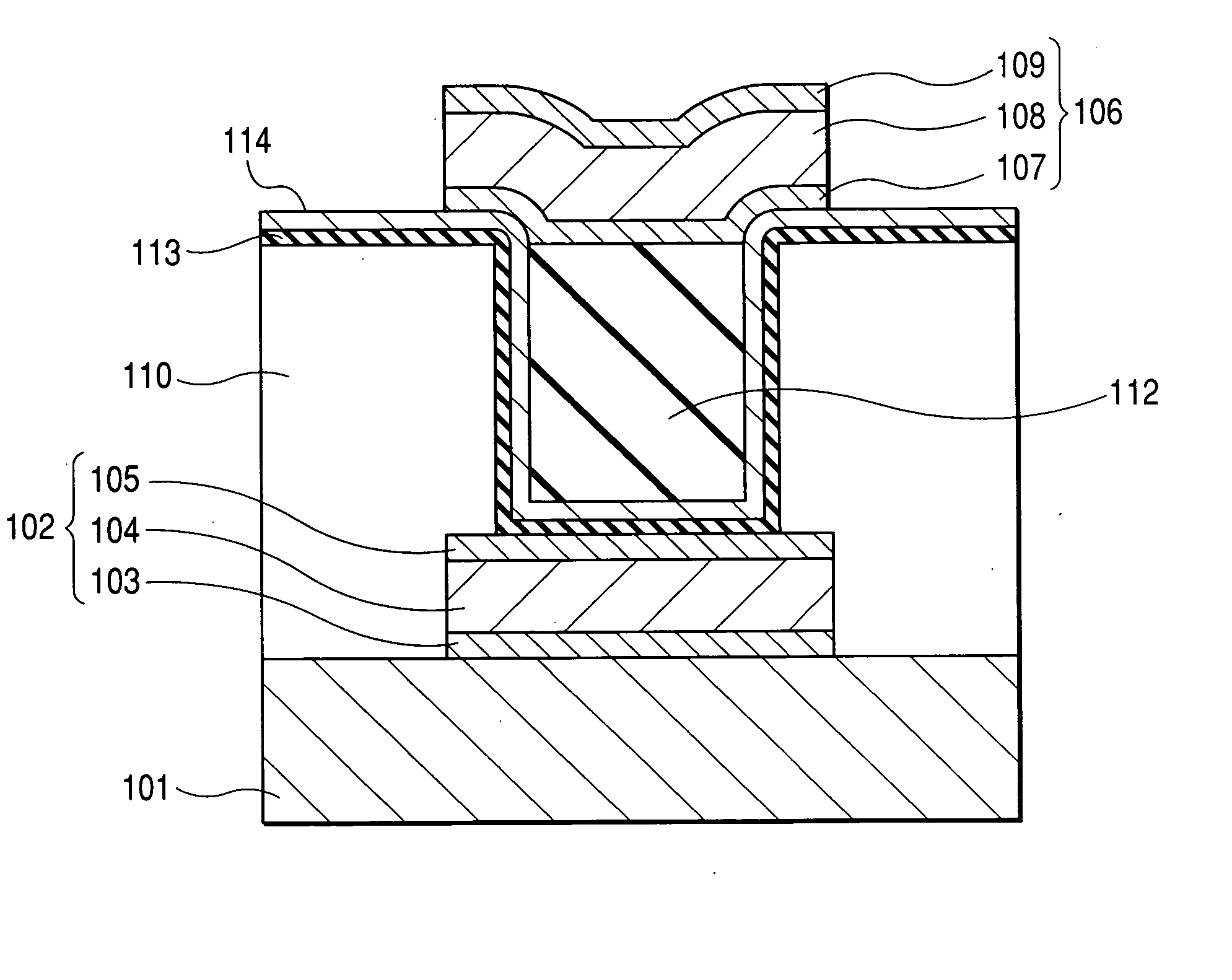
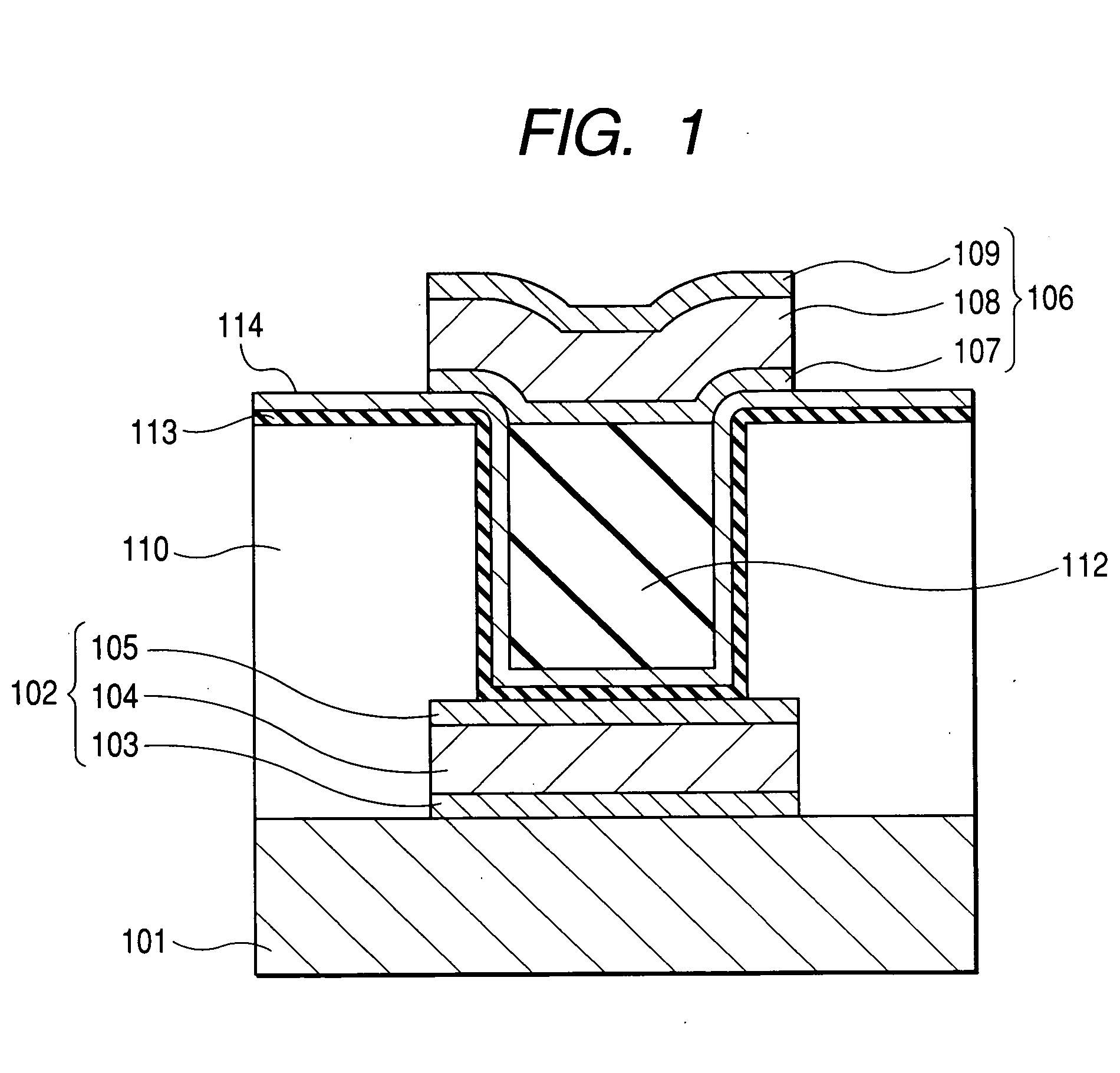
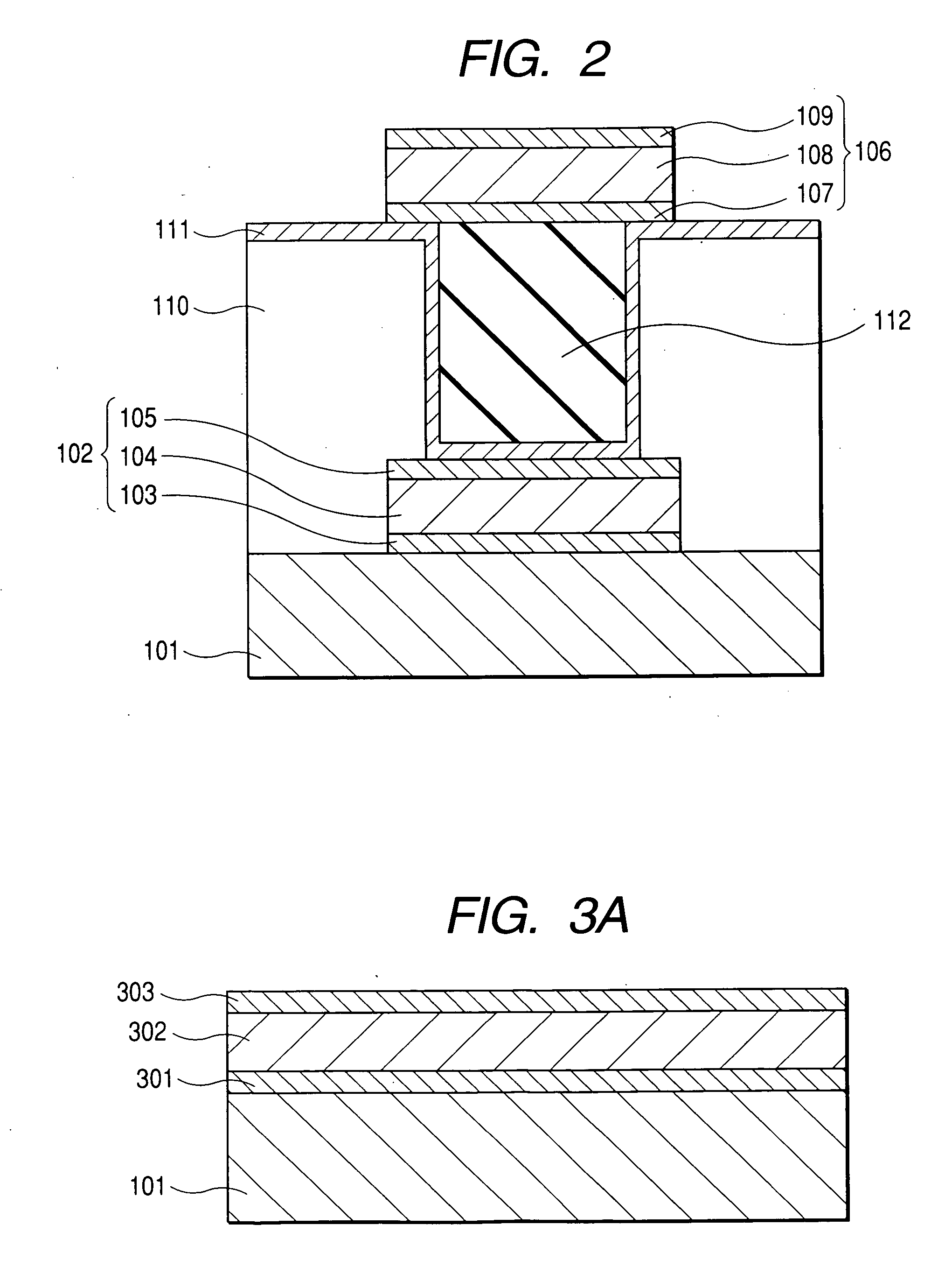
[0035]FIG. 1 is a sectional view of Embodiment 1 of the present invention. A first wiring layer (102) is existent on a semiconductor substrate (101) having an active device formed thereon and consists of a metal layer (104) and upper and lower layers (103, 105) made of titanium nitride as a barrier metal. A second wiring layer (106) is existent above the first wiring layer and consists of a metal layer (108) and upper and lower layers (107, 109) made of a barrier metal. An ordinary interlayer dielectric (110) is interposed between the two metal wiring layers, and an opening is formed in the interlayer dielectric in a portion which will become an MIM capacitor. An aluminum oxide layer (113) and a niobium oxide layer (114) are formed as capacitor dielectrics on the inner wall of the opening. The aluminum oxide layer (113) is an amorphous film having a thickness of 2 nm and the niobium oxide layer is a crystallized film having a thickness of 5 nm. The opening is filled with these capac...

embodiment 2

[0048] A lamination method according to another preferred embodiment of the present invention is disclosed next. Since the principle of the present invention is to carry out temperature correction with the film thickness ratio of aluminum oxide to niobium oxide, it is of no essential significance that aluminum oxide and niobium oxide disclosed in FIG. 1 and FIGS. 3A to 3G are deposited in the mentioned order. Niobium oxide may be deposited first. Further, FIG. 11 shows only the electrode / dielectric laminated structure of the capacitor shown in FIG. 1 which has a three-layer structure consisting of an aluminum oxide layer (401), niobium oxide layer (402) and aluminum oxide layer (403). Also in this case, the present invention can be carried out by setting the ratio of the total thickness of the upper and lower aluminum oxide layers (401, 403) to the thickness of the niobium oxide layer (402) to 0.2 to 1, preferably 0.4 to 0.7.

[0049] When a higher application voltage is used, the alu...

embodiment 3

[0050] Other preferred materials of the niobium oxide layer in the present invention are disclosed next. Although niobium oxide is a dielectric which can be crystallized at 300 to 400° C. specifically, out of simple oxides showing high insulating properties, when its insulation resistance is compared with those of other similar simple oxides, it is slightly lower. To improve this, tantalum oxide was mixed with niobium oxide. FIG. 13 shows the dependence upon mixing ratio of dielectric constant when the crystallization annealing of a mixed film deposited on the 2 nm-thick aluminum oxide film was carried out at 450° C. When the mixing ratio of tantalum oxide was 10% or less, the same dielectric constant as pure niobium oxide was obtained and the desired effect of increasing insulation resistance could be obtained. That is, the niobium oxide layer of the present invention can be mixed with tantalum oxide in a mixing ratio of 10% or less. Also in this case, the present invention can be ...


PUM


Abstract

An integrated semiconductor device comprising an analog integrated circuit or mixed signal integrated circuit having a capacitor, wherein the dielectric film of the capacitor is a laminated film consisting of a first dielectric film essentially composed of aluminum oxide and a second dielectric film essentially composed of crystallized niobium oxide. This integrated semiconductor device is small in size and has a low temperature coefficient and high reliability. The niobium oxide is crystallized to increase its dielectric constant and reduce its loss. To reduce the temperature coefficient, the film thickness ratio of the aluminum oxide layer to the niobium oxide layer is set to 0.2 to 1, preferably 0.4 to 0.7.

Description

CLAIM OF PRIORITY [0001] The present application claims priority from Japanese application JP 2004-359724 filed on Dec. 13, 2004, the content of which is hereby incorporated by reference into this application. FIELD OF THE INVENTION [0002] The present invention relates to an integrated semiconductor device and to a method of manufacturing the same and, particularly, to an integrated semiconductor device which can be reduced in size, experiences small changes in its characteristic properties caused by ambient temperature and operation conditions and has a highly reliable capacitor and to a method of manufacturing the same. BACKGROUND OF THE INVENTION [0003] In an integrated circuit for carrying out the analog processing of an electric signal, the values of a passive device such as capacitor, resistor or inductor are important factors for determining circuit operation, in addition to the characteristic properties of an active device typified by MOSFET. Heretofore, most of these passiv...

Claims


Application Information

Patent Timeline
IPC IPC(8): H01L29/00
CPCH01L21/31604H01L21/31616H01L21/76838H01L27/0805H01L28/56H01L28/90H01L21/02266H01L21/02274H01L21/02183H01L21/02178H01L21/022H01L21/02271H01L21/0228
Inventor MIKI, HIROSHI
Owner HITACHI LTD
Why Eureka
Try Eureka