Dual platform semiconductor laser device

a laser device and semiconductor technology, applied in semiconductor lasers, laser cooling arrangements, laser details, etc., can solve the problems of poor device yield rate, deterioration of laser components, and inability to meet high frequency operations of ion-implant vertical-cavity surface emitting lasers (vcsels), so as to facilitate the production of metal layers, improve surface planarization, and mechanical stress for wire bonding

Inactive Publication Date: 2006-06-15
TRUE LIGHT
View PDF9 Cites 0 Cited by
  • Summary
  • Abstract
  • Description
  • Claims
  • Application Information

AI Technical Summary

Benefits of technology

[0016] Further, the present invention is to provide a dual platform semiconductor laser device, wherein the second independent platform is formed directly on the semiconductor structure, so that the ion implant can adjust the capacitance as well as obtaining a higher mechanical stress for the wire bonding.
[0017] Another further, the present invention is to provide a dual platform semiconductor laser device, such that a dielectric material is filled between the exteriors of the dual platforms to form a dielectric layer for obtaining a better surface planarization and facilitating the production of the metal layer and lowering the connected metal capacitance.

Problems solved by technology

However, when the ion implant technology is used, its implant area cannot be too close to the active layer of the surface emitting laser, otherwise the high-energy particles may destroy the material of the active layer and deteriorate the properties of the laser components, and thus the ion-implant vertical-cavity surface emitting laser (VCSEL) is not suitable for high frequency operations.
After a device is selectively etched, the device will have a non-planarized surface which may produce a crack and cause a poor yield rate of the device, when the metal electrode is produced on a non-planarized surface.
Of course, the equipments and manufacturing costs will be more expensive.
However, the wire bonding area created by filling a dielectric material has a weaker mechanical stress due to the properties of the dielectric material.
As a result, films often cracks during the wire bonding process, and the effect of the wire bonding will be affected adversely, or even worse, the wire bonding cannot be completed.

Method used


Image

  • Dual platform semiconductor laser device
  • Dual platform semiconductor laser device
  • Dual platform semiconductor laser device

Examples


Embodiment Construction

[0023] The technical characteristics, features and advantages of the dual platform semiconductor laser device in accordance with the present invention will become apparent in the following detailed description of the preferred embodiments with reference to the accompanying drawings.

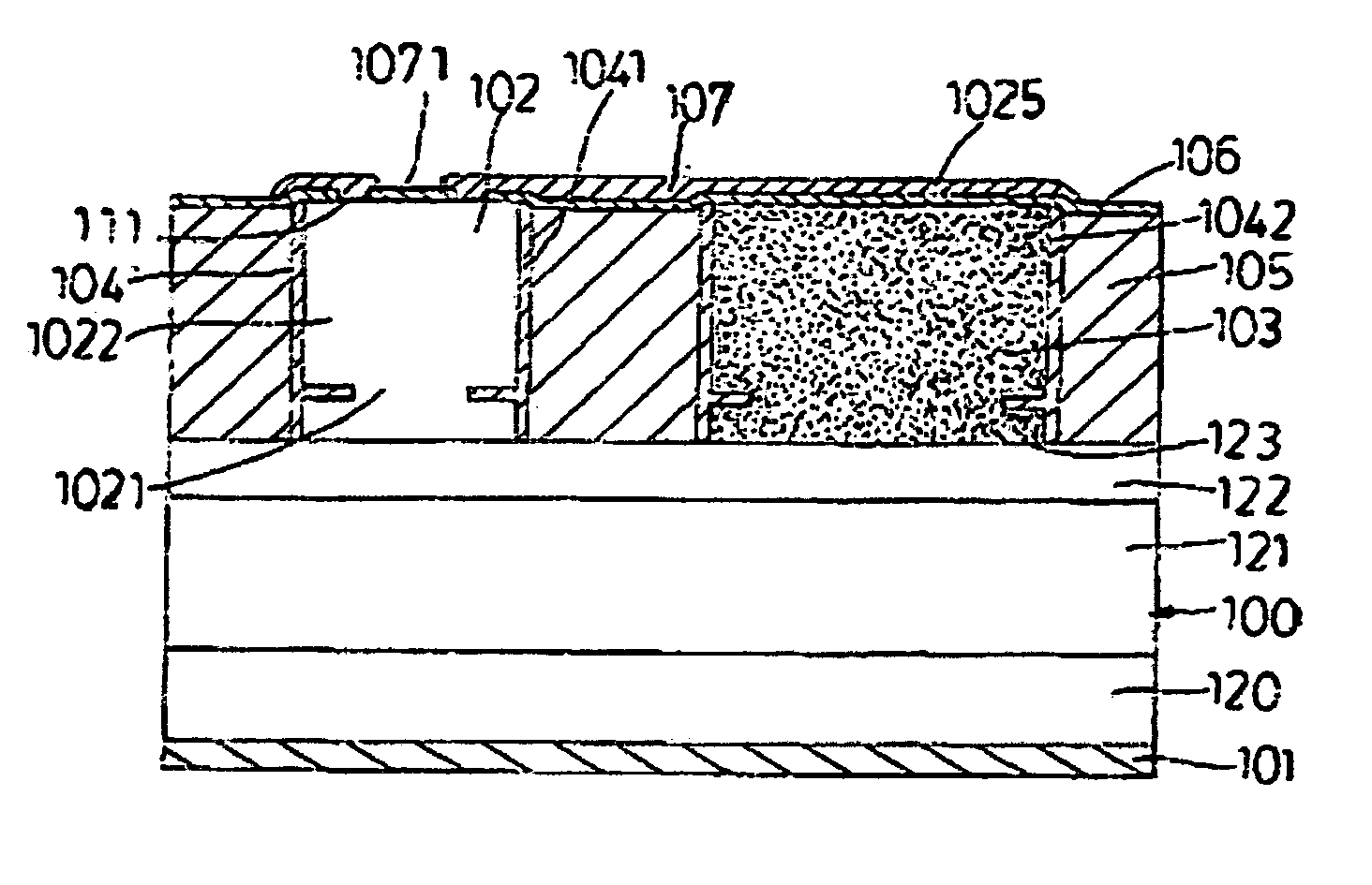
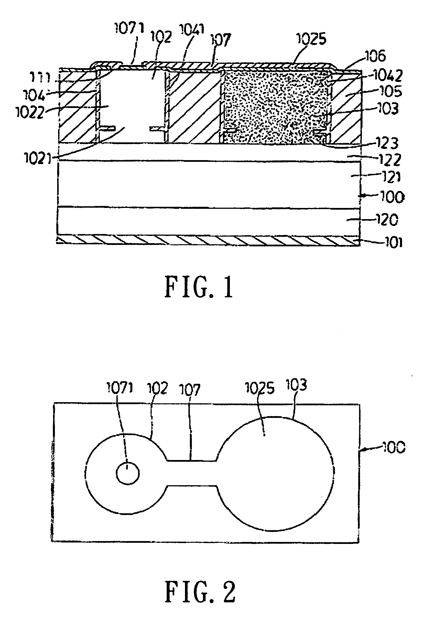
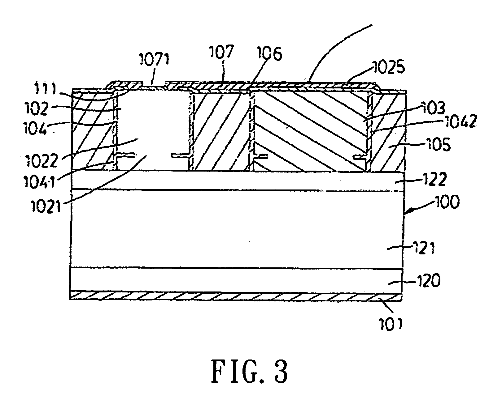
[0024] Referring to FIGS. 1 and 2 for the lateral cross-sectional view and the top view of a dual platform semiconductor laser device according to a preferred embodiment of the present invention, the dual platform semiconductor laser device of the invention comprises a laser chip layer (VCSEL) 100, a bottom electrode layer 101 (with a cathode layer), a first independent platform 102, a second independent platform 103, an oxide layer 104, a dielectric layer 105, a protective layer 106 having a contact area hole 111 and a metal layer 107. From the bottom up, there are a bottom electrode layer 101, a laser chip layer (VCSEL) 100, a light emitting active area platform 102, a wire bonding area platform 103, a...


PUM


Abstract

A dual platform semiconductor laser device includes a laser chip layer, two independent platforms formed on the laser chip layer and defining a light emitting active area platform and a wire bonding platform, a planarized dielectric layer filled between the independent platforms, a protective layer disposed at the dielectric layer and including a contact area hole corresponding to the first independent platform, coated onto the metal layer at the protective layer and coupled to the first independent platform, and extended to the second independent platform to form a pad for wire bonding the first independent platform. The independent platforms define the second independent platform for wire bonding, and its capacitance is modulated to provide a stronger wire bonding strength, and the dielectric layer filled at the external sides of the two platforms lowers the wire connected metal capacitance and obtain a planarized surface for producing the metal layer easily.

Description

BACKGROUND OF THE INVENTION [0001] 1. Field of the Invention [0002] The present invention relates to a dual platform semiconductor laser device, and more particularly to a technical area that relates to an oxide confined vertical-cavity laser having a dual platform semiconductor structure. [0003] 2. Description of Prior Art [0004] Optical information and communication systems provide a major method for moving huge data in a high speed, and one of the main components of such optical information and communication systems is an optical transceiver. At the data transmitting end, an optical transceiver is provided for translating a data in the form of electric signals (such as a digital data in the form of 0 and 1) into an optical signal which is suitable to be transmitted by a transmission medium (such as an optical fiber cable). At the data receiving end, the optical transceiver translates the received optical signal back into a data in the form of electric signals. One of the major co...

Claims


Application Information

Patent Timeline
Patent Type & Authority Applications(United States)
IPC IPC(8): H01S5/00
CPCH01S5/0261H01S5/0425H01S5/06226H01S5/18311H01S5/2214H01S2301/176H01S5/04254
Inventor LEE, BORLINWU, CHUN-HANPAN, JIN-SHANLAI, HUNG-CHING
Owner TRUE LIGHT
Why Eureka
Try Eureka