Optical disk and its manufacturing method
a technology of optical disks and manufacturing methods, applied in the field of optical disks, can solve the problems of inability to absorb pressure, inability to react with bisphenol a, and remained unreacted, and achieve the effects of low substrate warpage, low cost, and high-definition images
- Summary
- Abstract
- Description
- Claims
- Application Information
AI Technical Summary
Benefits of technology
Problems solved by technology
Method used
Image
Examples
example 1
[0160] (Fabrication of Printing Sheet)
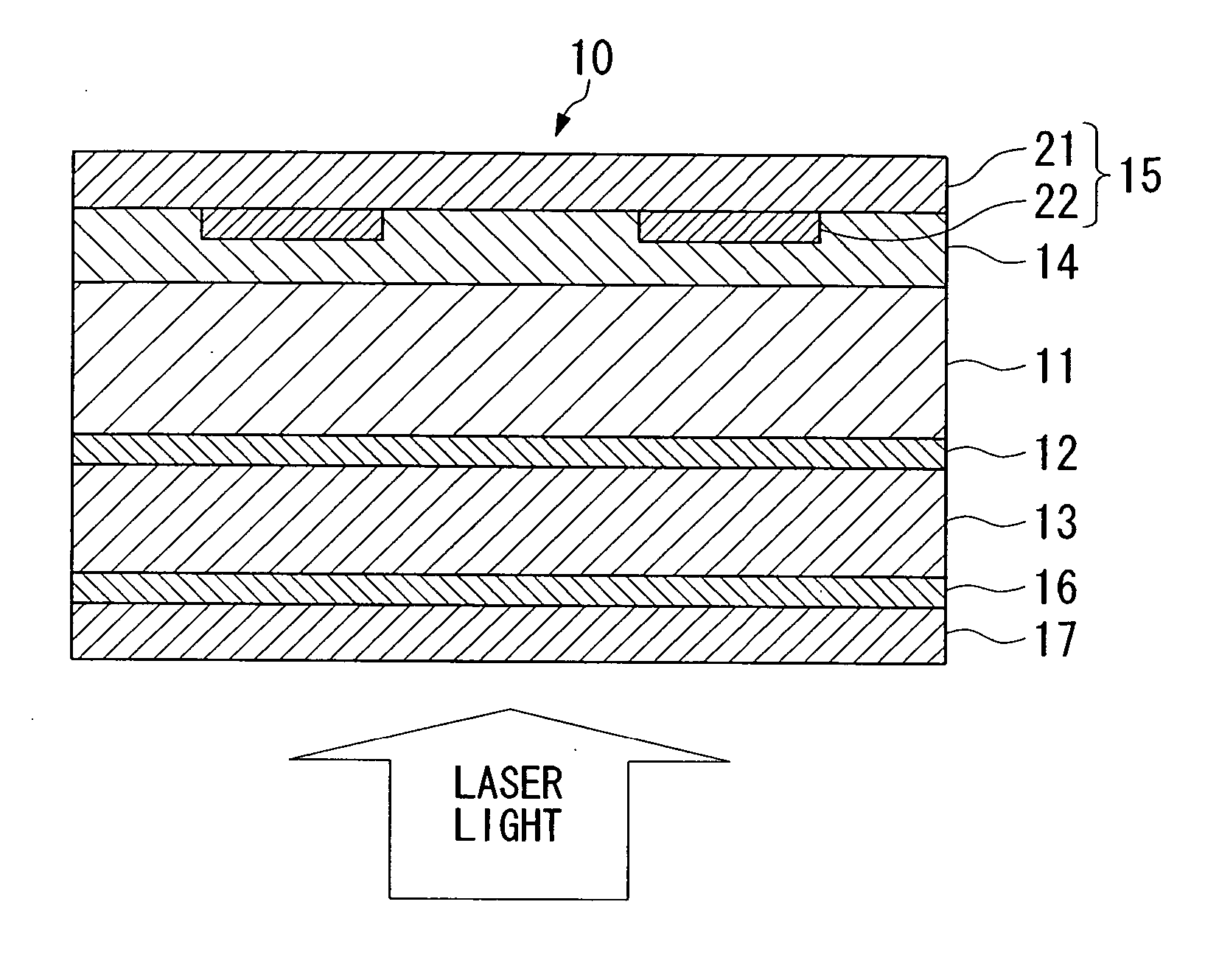
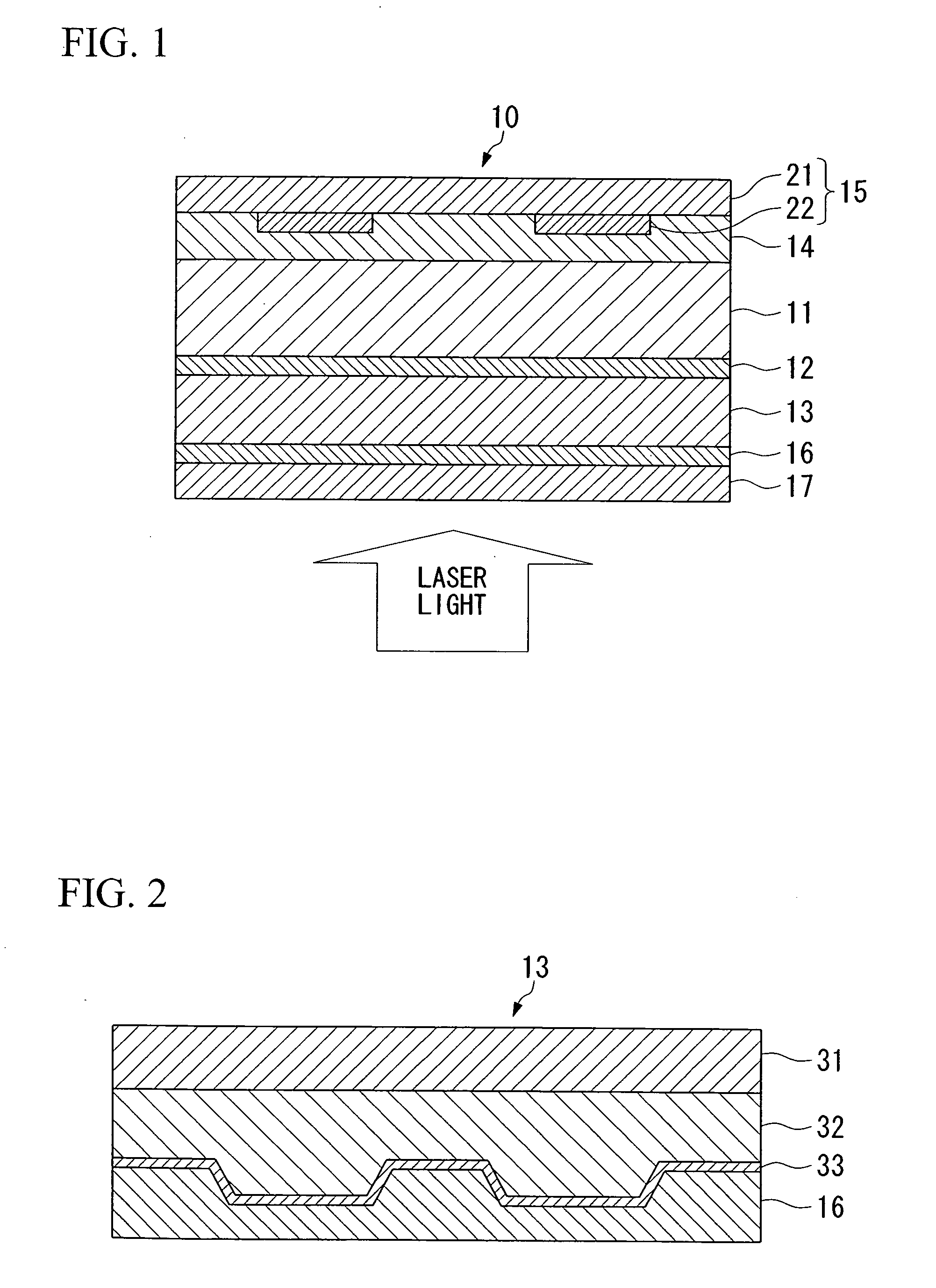
[0161] Gravure printing was carried out using biodegradable polyester printing ink (Dainichiseika Color and Chemicals, Biotech Color HGP) on a polylactic acid film drawn to a thickness of 0.04 mm (Mitsubishi Plastics, Ecoloju) to obtain a printing sheet on which was printed markings indicating the type of optical disk, additional information relating to the optical disk, decorative images and so forth.
[0162] (Fabrication of Substrate Sheet)
[0163] Polyethylene was molten extrusion coated onto both sides of resin-impregnated paper having a thickness of 1.0 mm (Hokuetsu Paper Mills, water-resistant vulcanized fiber) followed by preliminarily forming a release layer having a thickness of 0.015 mm.
[0164] (Fabrication of Recording Layer Sheet)
[0165] Surface irregularities corresponding to tracks and information pits were transferred to a copper-plated roll after which the roll was chrome-plated from above to obtain a transfer mold.
[0166] An ultr...
example 2
[0178] With the exception of changing the fabrication of the recording layer sheet as described below, optical disks were obtained in the same manner as Example 1.
[0179] (Fabrication of Recording Layer Sheet)
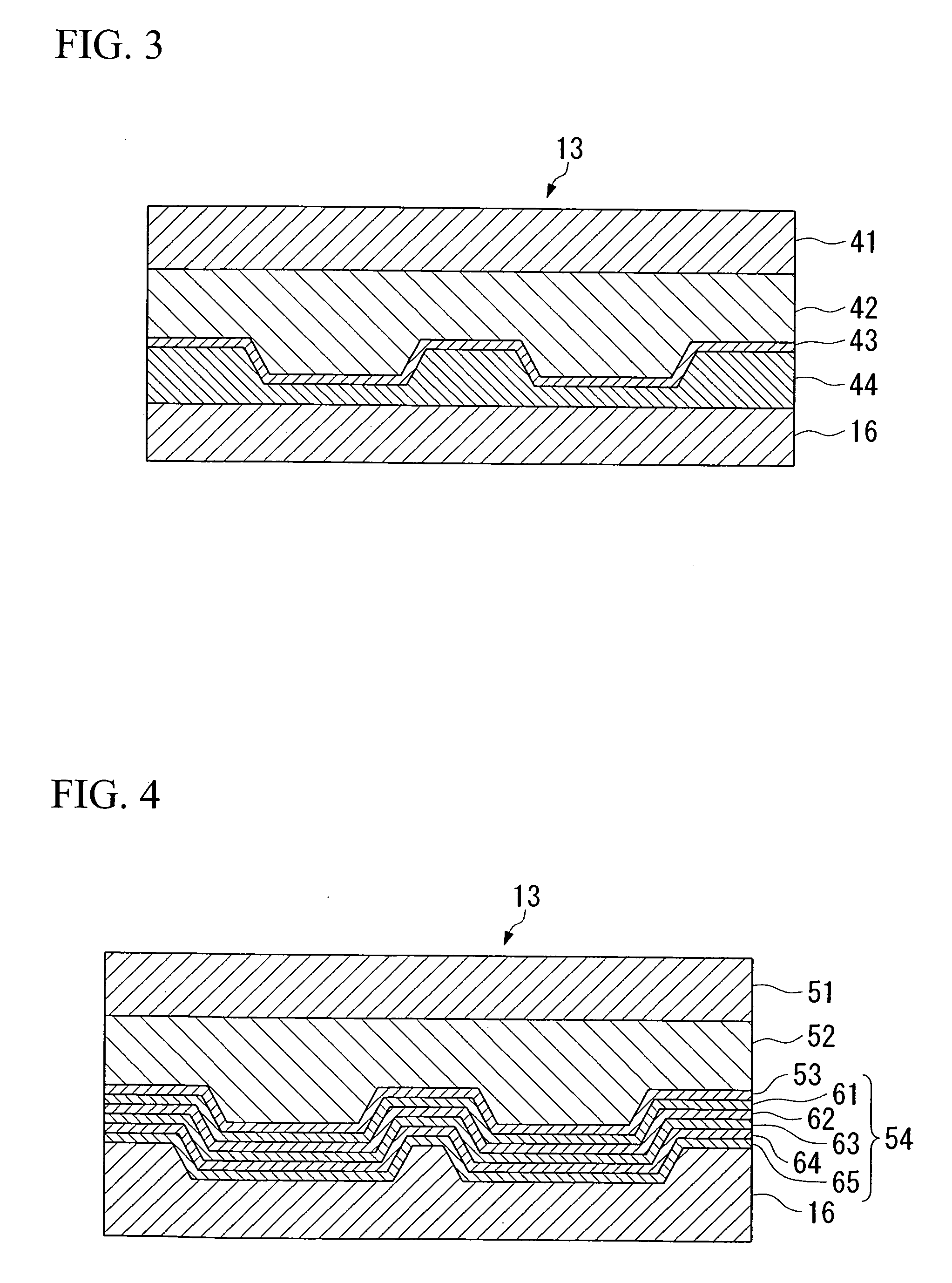
[0180] Surface irregularities corresponding to tracks and information pits were transferred to a copper-plated roll after which the roll was chrome-plated from above to obtain a transfer mold.
[0181] An ultraviolet-cured resin was coated onto a high-density polyethylene film drawn to a thickness of 0.05 mm with a die coater to a thickness of 0.1 mm, and the transfer mold was pressed against its surface to transfer the surface irregularities to the surface of the ultraviolet-cured resin.
[0182] Next, the ultraviolet-cured resin was irradiated with ultraviolet light to cure the ultraviolet-cured resin and form tracks.
[0183] Next, aluminum was vacuum deposited on the tracks and a light reflecting layer having a thickness of 60 nm was formed.
example 3
[0188] With the exception of changing the fabrication of the recording layer sheet as described below, optical disks were obtained in the same manner as Example 1.
[0189] (Fabrication of Recording Layer Sheet)
[0190] Surface irregularities corresponding to tracks were transferred to a copper-plated roll after which the roll was chrome-plated from above to obtain a transfer mold.
[0191] An ultraviolet-cured resin was coated onto a high-density polyethylene film drawn to a thickness of 0.05 mm with a die coater to a thickness of 0.1 mm, and the transfer mold was pressed against its surface to transfer the surface irregularities to the surface of the ultraviolet-cured resin.
[0192] Next, the ultraviolet-cured resin was irradiated with ultraviolet light to cure the ultraviolet-cured resin and form tracks.
[0193] Next, aluminum was vacuum deposited on the tracks and a light reflecting layer having a thickness of 60 nm was formed.
[0194] Next, an SiO2 film having a thickness of 220 nm, a ...
PUM
| Property | Measurement | Unit |
|---|---|---|
| roughness Rmax | aaaaa | aaaaa |
| roughness Rmax | aaaaa | aaaaa |
| thickness | aaaaa | aaaaa |
Abstract
Description
Claims
Application Information


