Dye sensitization photoelectric converter and process for producing the same

a photoelectric converter and dye sensitization technology, applied in the direction of electrochemical generators, sustainable manufacturing/processing, final product manufacturing, etc., can solve the problems of concrete guide line for forming a complex, high economic cost and energy cost in a manufacturing process, and reduce energy conversion efficiency, so as to improve energy conversion efficiency

Inactive Publication Date: 2006-06-29
SONY CORP
View PDF42 Cites 36 Cited by
  • Summary
  • Abstract
  • Description
  • Claims
  • Application Information

AI Technical Summary

Benefits of technology

[0020] Namely, since the transfer of the charge carrier after being injected in the semiconductor layer is controlled based on the energy level of the passage, through which the charge carrier is transferred, in the semiconductor layer, in comparison with a case in which the transfer of the charge carrier is relied on a diffusive migration, the number of the charge carriers which can reach the electrode from which the charge carriers are drawn out is increased, to thereby enhance the energy conversion efficiency.

Problems solved by technology

The solar cell which utilizes a pn junction of a semiconductor is most widely distributed, but, since it is necessary to conduct a step of manufacturing a semiconductor material of high purity or a step of forming the pn junction, there is a problem in that an economical cost and an energy cost in a manufacturing process are high.
Since these electrons can not be drawn out as an electric current, the electrons cause a reduction of energy conversion efficiency.
However, a concrete guide line for forming a complex while taking an energy level of the semiconductor into consideration has not yet been established.

Method used


Image

  • Dye sensitization photoelectric converter and process for producing the same
  • Dye sensitization photoelectric converter and process for producing the same
  • Dye sensitization photoelectric converter and process for producing the same

Examples


embodiment 1

A Case in Which Semiconductor Layers Having Different Band Structures From One Another are Laminated

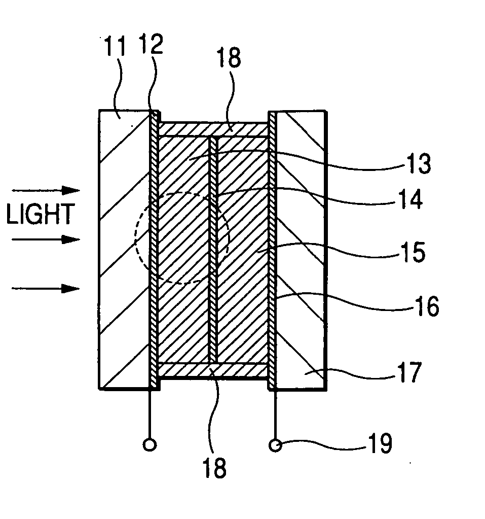
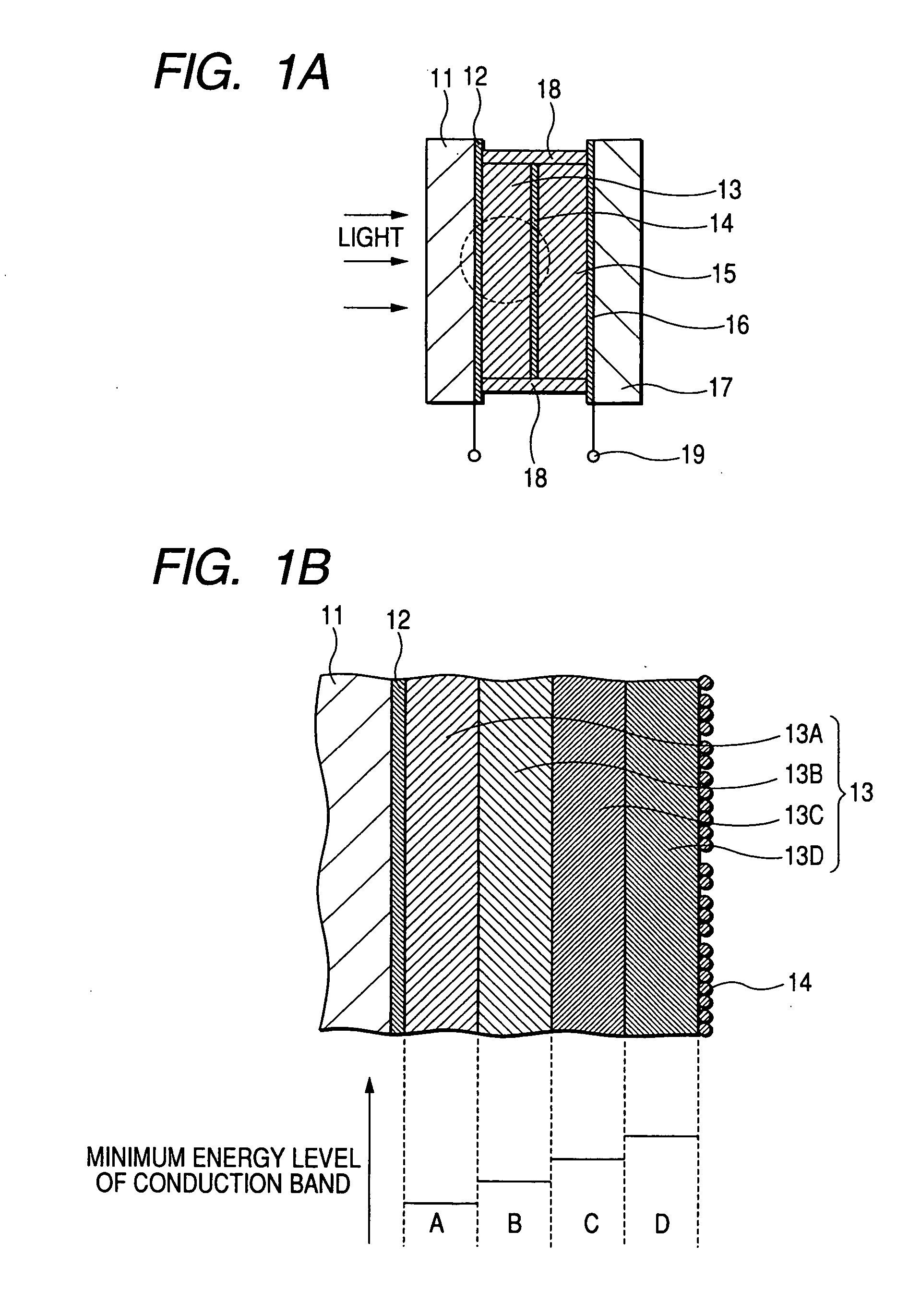
[0043]FIGS. 1A and 1B are a schematic cross-sectional diagram of an illustrative example of a dye-sensitized photochemical cell according to Embodiment 1 and an enlarged cross-sectional view of a major portion thereof taken along a broken line in the schematic cross-sectional diagram, respectively.

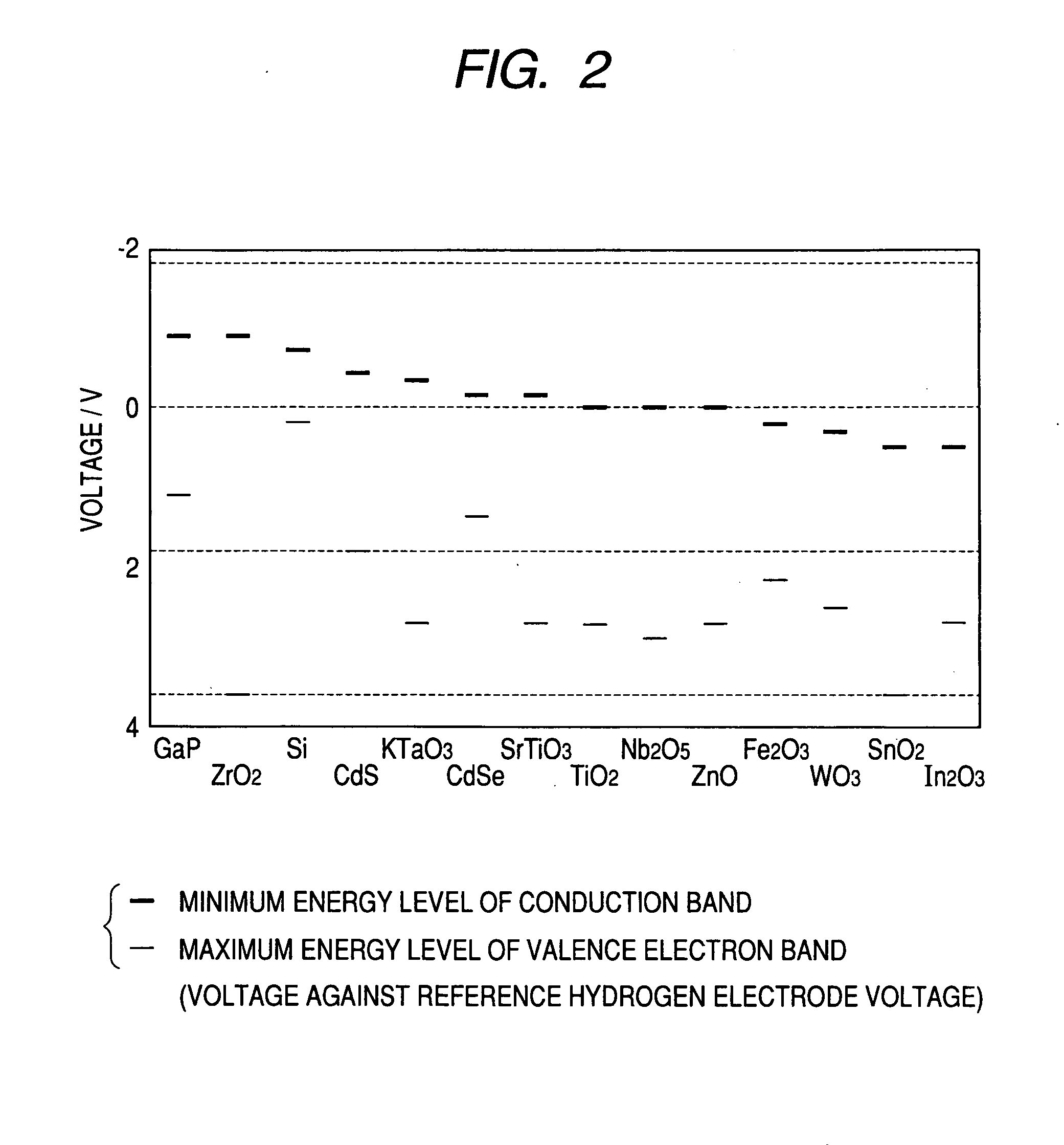
[0044] A transparent substrate 11 is a material having such a property and a shape as allow light to be easily transmitted; for example, a glass sheet or a transparent plastic sheet made of, for example, polyethylene terephthalate or polycarbonate is used. Since it is not necessary that the other substrate 17 is transmittable to light, an opaque glass sheet, a plastic sheet, ceramic sheet or metal sheet may be used.

[0045] On a surface of the transparent substrate 11, a transparent electrode 12 is formed as an electrode (negative electrode) for drawing an electron out. A material of the tr...

embodiment 2

A Case in Which Semiconductor Superfine Grains Having Different Band Structures From One Another are Laminated

[0057]FIG. 3 is an enlarged cross-sectional view of a major portion of a negative electrode according to Embodiment 2 of the invention. A schematic cross-sectional view of an entire dye-sensitized photochemical cell is same as in Embodiment 1 as shown in FIG. 1A and, accordingly, omitted.

[0058] In Embodiment 1, a case in which thin films of the semiconductor materials are laminated one on the other is shown, but, in Embodiment 2, a process comprising coating of a dispersion in a paste state containing superfine grains of the semiconductor material, evaporating of a dispersion medium and sintering of the superfine grains is repeatedly performed on a plurality of semiconductor materials, to thereby produce a laminate structure.

[0059] In a same manner as in Embodiment 1, by laminating a plurality of semiconductor materials having different band structures from one another on...

embodiment 3

A Semiconductor Layer (1) Comprising a Complex of a Titanium Oxide Thin Film Having a Drift Region of an Electron Inside and a Titanium Oxide Fine Grain

[0079] Hereinafter, with reference to FIGS. 4A to 4G, a manufacturing process of a semiconductor layer 33 comprising a complex of a titanium thin film having a drift region of an electron inside and a titanium oxide fine grain will be described.

Step 1

[0080] A thin film electrode 32 is formed on a surface of a substrate 31. As for the substrate 31, for example, a glass sheet is used. The thin film electrode 32 is, for example, a thin film of indium oxide doped with tin (ITO) or gold and is formed by a vapor deposition or sputtering.

Step 2

[0081] A TiO2 thin film 41 is formed on the substrate 31. Such film forming may be performed by sputtering or, otherwise, may be performed by a sol-gel method.

[0082] When the substrate 31 is titanium Ti, a TiO2 layer 41 may be formed by using an anodic oxidation coating.

Step 3

[0083] An impu...


PUM

PropertyMeasurementUnit
Thicknessaaaaaaaaaa
Thicknessaaaaaaaaaa
temperatureaaaaaaaaaa

Abstract

A dye-sensitized photoelectric conversion apparatus having enhanced energy conversion efficiency and a production method thereof are provided. The dye-sensitized photoelectric conversion apparatus which has semiconductor layer (13) containing a photosensitizing dye (14) and is constituted such that a charge carrier generated by allowing light to incident in the photosensitizing dye (14) is drawn out through the semiconductor layer (13), in which the semiconductor layer (13) is constituted by a plurality of regions (13A to 13D) having different energy levels from one another of a passage through which the charge carrier is transferred. Further, the plurality of regions (13A to 13D) are arranged such that the energy levels are reduced stepwise and / or continuously in the direction of drawing the charge carrier out.

Description

TECHNICAL FIELD [0001] The present invention relates to a dye-sensitized photoelectric conversion apparatus applicable to a solar cell and the like and a manufacturing method thereof. BACKGROUND ART [0002] A solar cell utilizing sunlight is receiving attention as an energy source that can substitute for a fossil fuel, and various types of studies have been exerted. The solar cell is one type of photoelectric conversion apparatus which can convert light energy into electric energy. [0003] The solar cell which utilizes a pn junction of a semiconductor is most widely distributed, but, since it is necessary to conduct a step of manufacturing a semiconductor material of high purity or a step of forming the pn junction, there is a problem in that an economical cost and an energy cost in a manufacturing process are high. [0004] On the other hand, a dye-sensitized photochemical cell which utilizes a light-excited electron transfer has been proposed by Graetzel et al. (Japanese Patent No. 26...

Claims


Application Information

Patent Timeline
Patent Type & Authority Applications(United States)
IPC IPC(8): H01L31/00H01L31/04H01G9/20H01M14/00
CPCH01G9/2031H01G9/2059H01M14/005Y02E10/542Y02P70/50H01L31/04H01L31/18H01M14/00
Inventor IMOTO, TSUTOMUODA, MASAO
Owner SONY CORP
Why Eureka
Try Eureka