Semiconductor optical converter

a technology of semiconductor parts and optical converters, applied in optics, instruments, nanotechnology, etc., can solve the problems of deteriorating waveform of optical signals transmitted through optical fibers, and affecting the performance of optical converters. achieve the effect of high efficiency

Active Publication Date: 2006-07-20
NIPPON TELEGRAPH & TELEPHONE CORP
View PDF4 Cites 15 Cited by
  • Summary
  • Abstract
  • Description
  • Claims
  • Application Information

AI Technical Summary

Benefits of technology

[0047] By employing the structures according to the first to fifth aspects of the present invention, the semiconductor Mach-Zehnder type optical modulator of the present invention can realize a traveling-wave-type electrode structure that can generate a refractive-index modulation by an electric field with high efficiency.

Problems solved by technology

However, the electroabsorption optical modulator is characterized in that the waveform of an optical signal that has been transmitted through an optical fiber is deteriorated owing to wavelength chirping caused when modulated.
As a result, transmission characteristics are deteriorated.
However, the lumped-constant type modulator has a great optical loss in the p-type semiconductor part.
Additionally, the lumped-constant type modulator has difficulty in performing an operation at 10 Gbit / s or more because of speed restrictions by the CR time constant.
The conventional lumped constant type modulator having the pin structure has proved difficult in realizing a traveling-wave-type electrode structure because of the waveguide loss of an electric signal in the p-type electrode and because of mismatching in velocity between light and an electric field caused by the capacity component of the pin structure.
However, it is difficult to steeply control an n-type carrier concentration and a p-type carrier concentration at a layer interface.
Therefore, it is very difficult to produce a practical optical modulator that employs the BRAQWET structure.
However, since low-temperature growth GaAs (LTG-GaAs) is used as high-resistance GaAs, optical losses are generated by a fault caused by the low-temperature growth.
As described above, among the semiconductor Mach-Zehnder type optical modulators being presently researched, the lumped-constant type modulator proves difficult in operating at 10 Gbit / s or more because the optical loss is great in the p-type semiconductor part, and speed restrictions by the CR time constant are imposed.
The traveling-wave-electrode-type modulator has a problem in the fact that the modulation efficiency of the refractive index is small, and the phase-modulating portion cannot be easily reduced in size, so that an operating voltage becomes high.

Method used


Image

  • Semiconductor optical converter
  • Semiconductor optical converter
  • Semiconductor optical converter

Examples


first embodiment

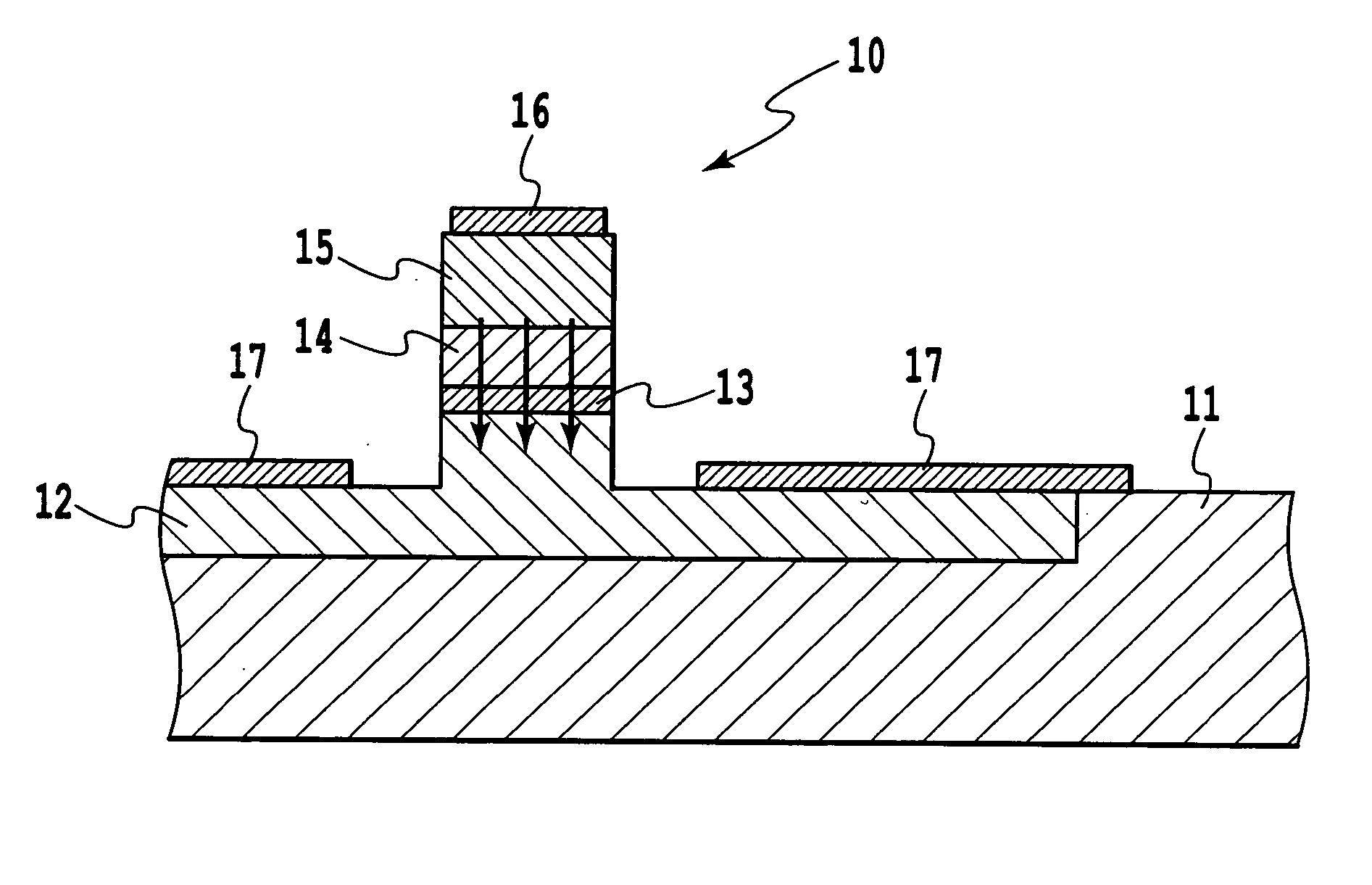
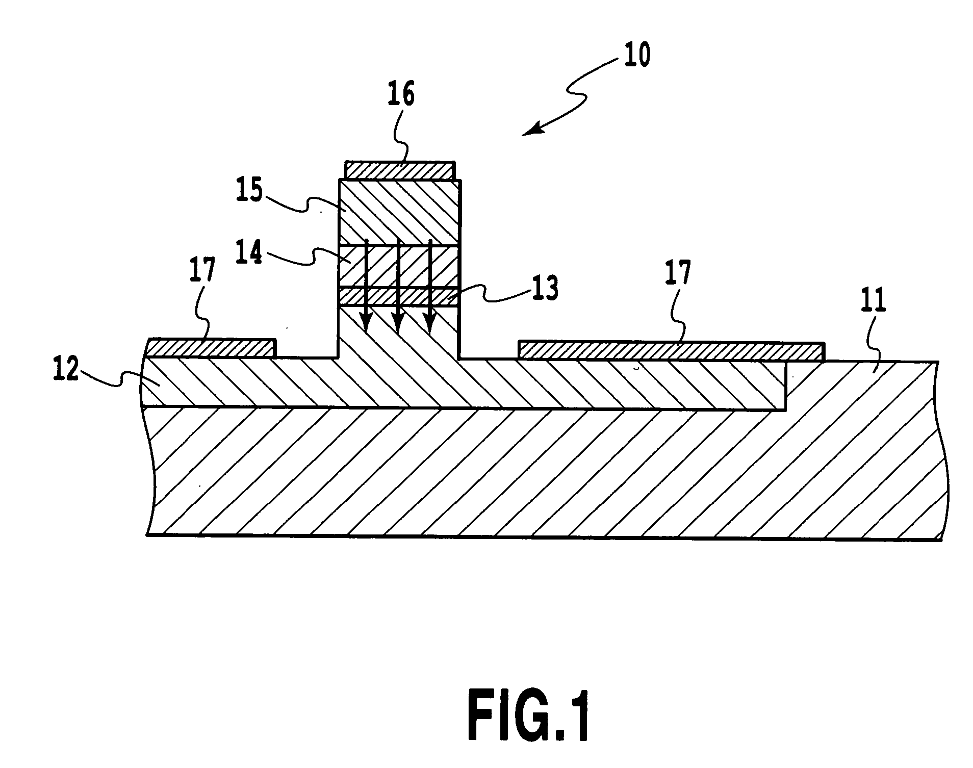
[0071]FIG. 1 is a schematic sectional view of a waveguide of an InP-based multi-quantum well semiconductor optical modulator according to a first embodiment, showing a cross-sectional structure of a part, to which an electric field is applied, of the waveguide.

[0072] The semiconductor optical modulator according to this embodiment has an optical waveguide structure obtained by processing a layered structure, in which an n-InP cladding layer 12, an optical waveguide core layer 13, an SI-InP cladding layer 14, and an n-InP cladding layer 15 are sequentially laminated on an SI-InP substrate 11, so as to be shaped like a mesa according to an etching process.

[0073] The semiconductor optical modulator according to the first embodiment is a high-mesa waveguide structure 10 in which an etching operation is applied to a part under the optical waveguide core layer 13 (in this embodiment, to the n-InP cladding layer 12 that is a layer placed under the optical waveguide core layer 13).

[0074]...

second embodiment

[0091]FIG. 5 shows a schematic external appearance of a Mach-Zehnder type optical modulator according to a second embodiment. As shown in FIG. 5, the Mach-Zehnder type optical modulator 60 includes a 2×2 multi-mode interference (MMI) type coupler 68a that is used to divide input light into two light beams, two phase modulating waveguides 69a and 69b that modulate the phase of each of the divided light beams based on an applied voltage, a 2×2 multi-mode interference type coupler 68b that combines modulated light beams together, a signal electrode 66 used to apply an electric field to the phase modulating waveguides 69a and 69b, and a ground electrode 67, which are formed on a substrate. Herein, the length (phase modulation region) L of each of the phase modulating waveguides 69a and 69b is 3 mm.

[0092]FIG. 6 shows a cross-section of a phase modulating waveguide of the Mach-Zehnder type optical modulator according to the second embodiment. As shown in FIG. 6, the Mach-Zehnder type opt...

third embodiment

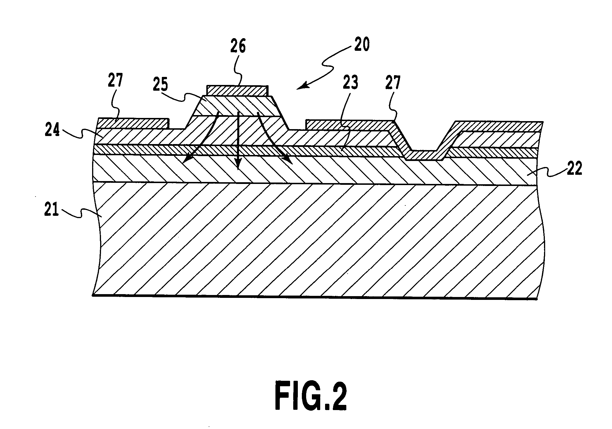
[0116]FIG. 11 is a schematic sectional view of a waveguide of an InP-based multi-quantum well semiconductor optical modulator according to a third embodiment. FIG. 11 shows a cross-sectional structure of an electric-field-applied portion of the waveguide.

[0117] The semiconductor optical modulator according to the third embodiment has an optical waveguide structure obtained by processing a layered structure, in which an n-InP cladding layer 42, an SI-InP cladding layer 48, an optical waveguide core layer 43, an SI-InP cladding layer 44, and an n-InP cladding layer 45 are sequentially laminated on an SI-InP substrate 41, so as to be shaped like a mesa according to an etching process.

[0118] The semiconductor optical modulator according to the third embodiment differs from the modulator according to the first embodiment in the fact that the layered structure is formed such that the SI-InP cladding layer 48 is placed between the optical waveguide core layer 43 and the n-InP cladding la...


PUM

PropertyMeasurementUnit
thicknessaaaaaaaaaa
lengthaaaaaaaaaa
lengthaaaaaaaaaa

Abstract

A semiconductor optical converter for use principally in an optical communications system or an optical information processing system.
The semiconductor optical converter comprises an n-InP clad layer (12), an optical waveguide layer (13), an SI-InP clad layer (14), and an n-InP clad layer (15) formed sequentially on an SI-INP substrate (11), characterized in that a voltage is applied from an electrode (16) connected with the n-InP clad layer (15) and ground electrode (17) connected with the n-InP clad layer (12). The semiconductor optical converter is especially applicable as a semiconductor phase modulator or a semiconductor Mach-Zehnder phase modulator operating at low voltages and having a low waveguide loss.

Description

TECHNICAL FIELD [0001] This invention relates to a semiconductor optical modulator, and in particular to a semiconductor optical modulator that can be used as a semiconductor phase modulator or a semiconductor Mach-Zehnder type optical modulator. BACKGROUND ART [0002] A waveguide type light control device, such as an optical modulator, is a key element in a high-speed optical communications system and an optical information processing system. The optical modulator includes, for example, an optical modulator that uses dielectric materials, such as LiNbO3 (LN), and an optical modulator that uses semiconductor materials, such as InP and GaAs. Among these optical modulators, expectations have been placed on a semiconductor optical modulator that can be integrated with other optical elements and other electronic circuits, such as lasers and optical amplifiers, and that can easily achieve a reduction in size and a reduction in voltage. [0003] An electroabsorption optical modulator and a M...

Claims


Application Information

Patent Timeline
Patent Type & Authority Applications(United States)
IPC IPC(8): G02F1/01G02F1/017G02F1/025G02F1/225
CPCB82Y20/00G02F1/01708G02F1/2257G02F1/015
Inventor TSUZUKI, KENITO, TSUYOSHIIGA, RYUZO
Owner NIPPON TELEGRAPH & TELEPHONE CORP
Why Eureka
Try Eureka