Organic thin film transistor and manufacturing method thereof

a thin film transistor and organic technology, applied in the direction of thermoelectric device junction materials, semiconductor devices, electrical apparatus, etc., can solve the problems of poor coverage of the gate insulating film formed on the gate electrode, increase the leakage of the gate electrode, and achieve the effect of stable operation characteristics and low cos

Inactive Publication Date: 2006-07-27
CANON KK
View PDF6 Cites 23 Cited by
  • Summary
  • Abstract
  • Description
  • Claims
  • Application Information

AI Technical Summary

Benefits of technology

[0010] Another object of the present invention is to provide a technique of using as a gate electrode a conductor film provided on a substrate whose shape is unstable and whose flatness is low as compared with a silicon wafer, such as a substrate made of a glass epoxy resin.
[0011] Still another object of the present invention is to provide a low cost semiconductor device using a large number of transistors in which stable operating characteristics are obtained.
[0020] Also, it is possible to obtain a low cost semiconductor device using a large number of transistors in which stable operating characteristics.

Problems solved by technology

In particular, there is a problem in the case where an organic polymer material such as polyethylene terephthalate or polycarbonate having lower flatness than a silicon wafer is used for a substrate, or in the case where a glass epoxy resin to which a copper foil is added is used for a printed substrate.
Because the surface roughness is 10 times to 1000 times larger than that of the silicon wafer, a coverage of the gate insulating film formed on the gate electrode is bad at some locations to increase a gate leakage.
Therefore, a sufficient electric field effect is not obtained.
Further, in some cases, the mobility is reduced due to the surface roughness.
However, in a method of directly forming a transistor on a substrate whose shape is unstable and whose flatness is low as compared with the silicon wafer, such as a substrate made of a glass epoxy resin, sufficient findings to the surface roughness required on the surface of the gate electrode are not obtained.

Method used


Image

  • Organic thin film transistor and manufacturing method thereof
  • Organic thin film transistor and manufacturing method thereof
  • Organic thin film transistor and manufacturing method thereof

Examples


example 1

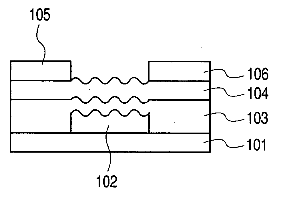
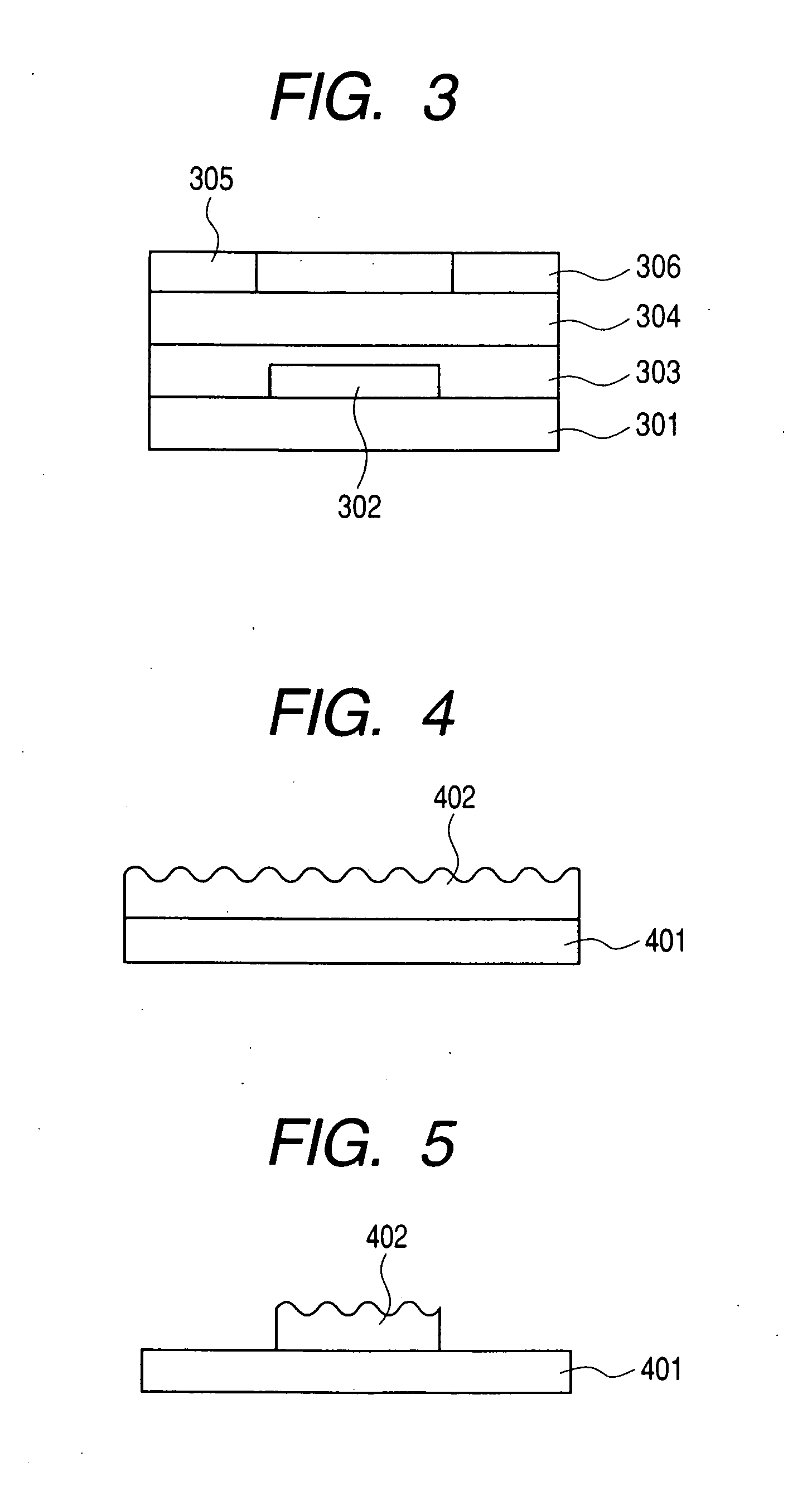
[0058] FIGS. 4 to 8 are schematic views showing a method of producing the organic thin film transistor according to the present invention. In FIG. 4, reference numeral 401 denotes a substrate and 402 denotes a conductor film. With respect to the substrate 401 and the conductor film 402, for example, a glass epoxy resin substrate which is integrally formed with a copper foil is commercially available as a printed circuit board. In this example, a substrate having a thickness of 0.2 mm in which a film thickness of the copper foil serving as the conductor film was 35 μm was used (produced by Hitachi Chemical Co., Ltd.; type: FR-4). A large number of substrates, each of which had a structure in which the conductor film was provided on both surfaces of the substrate. However, the conductor film provided on one surface is unnecessary on the description of the present invention and thus omitted here. The same reference numerals in FIGS. 4 to 8 indicate the same members.

[0059] Next, the co...

example 2

[0069] An organic thin film transistor was produced as in Example 1 except that polyethylene terephthalate (PET) was used for the substrate and gold was used for the gate electrode. With respect to the organic thin film transistor, a correlation between the average surface roughness Ra on the surface of the gate electrode and the incidence of defective products was examined.

[0070] The used PET was an OHP film whose thickness was 0.1 mm and size was A4. This was cut to a card side (86 mm×54 mm) as in Example 1.

[0071] A gold thin film which was to become the gate electrode was formed using a mask by resistance heating of tungsten boat in a vacuum evaporation system. In order to improve the contact of the gold thin film to the substrate, a thin chromium film was formed as a base layer. A thickness of the gold thin film was 0.5 μm and a thickness of the chromium film was 0.1 μm.

[0072] Next, a laminate of the chromium film and the gold thin film which was to become the gate electrode ...

example 3

[0074] A polyimide substrate having a thickness of 25 μm was used as the organic substrate. A copper foil having a thickness of 25 μm was grown on the substrate by plating. Four substrates each having the grown copper foil were prepared.

[0075] The four substrates were subjected to four types of surface processings, which were no polishing, soft etching processing, polishing tape processing, and CMP processing.

[0076] The conditions of the respective surface processing were as follows.

(Processing Conditions)

[0077] Soft etching processing: the substrate was immersed in 5% sulfuric acid for 30 seconds and then washed using flowing deionized water for 2 minutes. Tape processing: polishing tape (type: K8000); 60 second in polishing time; 1 m / 30 seconds in tape feed speed; and 2 kgf / cm2 in roll pressure. CMP processing: Shibaura slurry CHS-3000EM; 5 kg in cylinder pressure; 80 rpm in the number of revolutions of retainer and platen; and 25 minutes in polishing time.

[0078] The respect...


PUM


Abstract

There is provided an organic thin film transistor comprising: an organic substrate; a gate electrode; a gate insulating film; an organic semiconductor film; a source electrode; and a drain electrode, and in the organic thin film transistor, an average surface roughness Ra of the gate electrode which is in contact with the gate insulating film is 0.1 nm to 15 nm. The organic thin film transistor provides a stable performance characteristic even when a conductor film provided on a substrate whose shape is unstable and whose flatness is low as compared with a silicon wafer, such as a substrate made of a glass epoxy resin, is used as a gate electrode.

Description

TECHNICAL FIELD [0001] The present invention relates to an organic thin film transistor using an organic semiconductor material and a method of manufacturing the organic thin film transistor. BACKGROUND ART [0002] In recent years, a development race of a thin film transistor using an organic semiconductor material (hereinafter referred to as “organic thin film transistor”) is accelerating. By using the organic material, a process temperature is reduced. Therefore, it is expected that transistors can be formed on a large area at low cost. It is anticipated that organic thin film transistors will be applied to a drive circuit for a thin display and an electronic paper, a radio frequency identification (RF-ID) tag, an IC card, and the like. There are several technical reviews (see for example, C. D. Dimitrakopoulos, et al. “Organic Thin Film Transistors for Large Area Electronics”, Advanced Material, 2002, 14, No. 2, pp. 99-117). [0003]FIG. 3 shows a structural example of an organic th...

Claims


Application Information

Patent Timeline
Patent Type & Authority Applications(United States)
IPC IPC(8): H01L29/08H01L35/24H01L51/00H01L51/05H01L51/40
CPCH01L51/0021H01L51/0516H01L51/0545H10K71/60H10K10/468H10K10/466
Inventor KOGANEI, AKIOMOROTA, TAKAMITSU
Owner CANON KK
Why Eureka
Try Eureka