Semiconductor device, electronic device, and method of manufacturing semiconductor device

a semiconductor device and electronic technology, applied in the direction of semiconductor devices, semiconductor/solid-state device details, electrical apparatus, etc., can solve the problem of inevitable increase in manufacturing costs, and achieve the effect of stable formation, reduced material loss and cost, and high performan

Inactive Publication Date: 2006-08-03
SEMICON ENERGY LAB CO LTD
View PDF24 Cites 4001 Cited by
  • Summary
  • Abstract
  • Description
  • Claims
  • Application Information

AI Technical Summary

Benefits of technology

[0023] In accordance with the present invention, a component such as a wiring or the like included in a semiconductor device, a display device, or the like can be stably formed with a d...

Problems solved by technology

Therefore, the manufacturing cost is inevitably increa...

Method used


Image

  • Semiconductor device, electronic device, and method of manufacturing semiconductor device
  • Semiconductor device, electronic device, and method of manufacturing semiconductor device
  • Semiconductor device, electronic device, and method of manufacturing semiconductor device

Examples


embodiment mode 1

[0062] Embodiment Mode 1 of the present invention will be described with reference to FIGS. 1A to 1C.

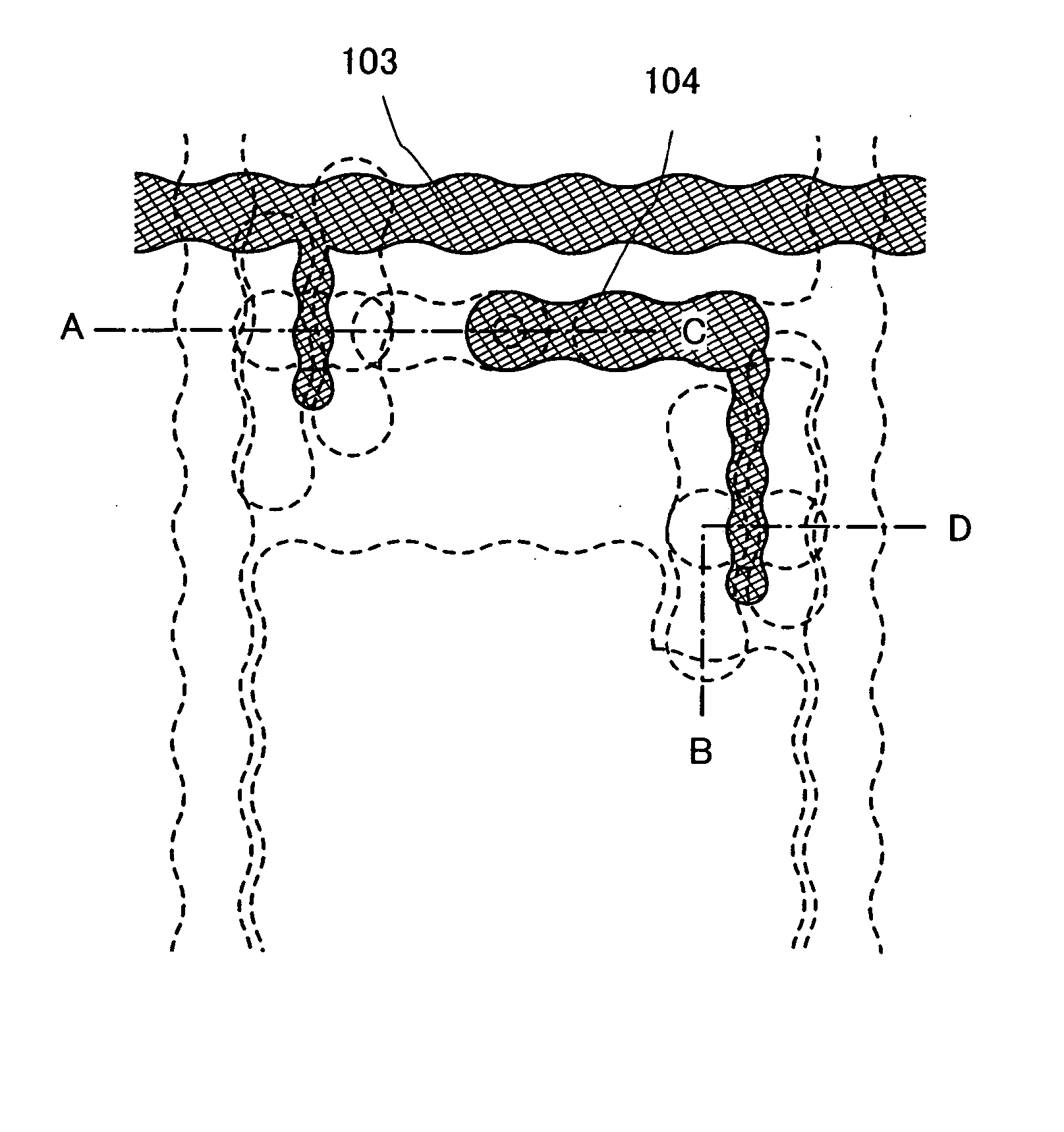
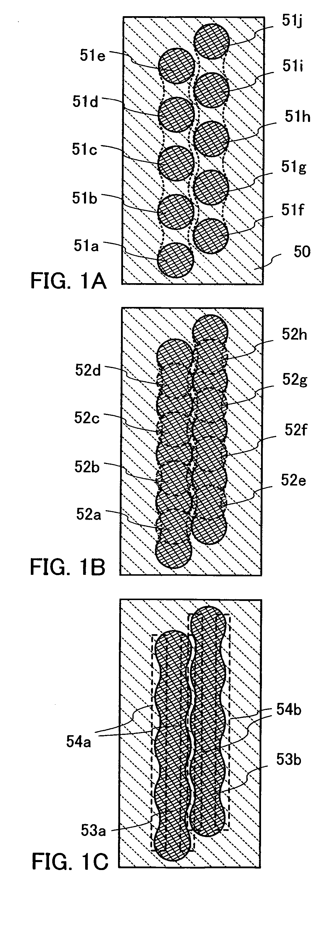
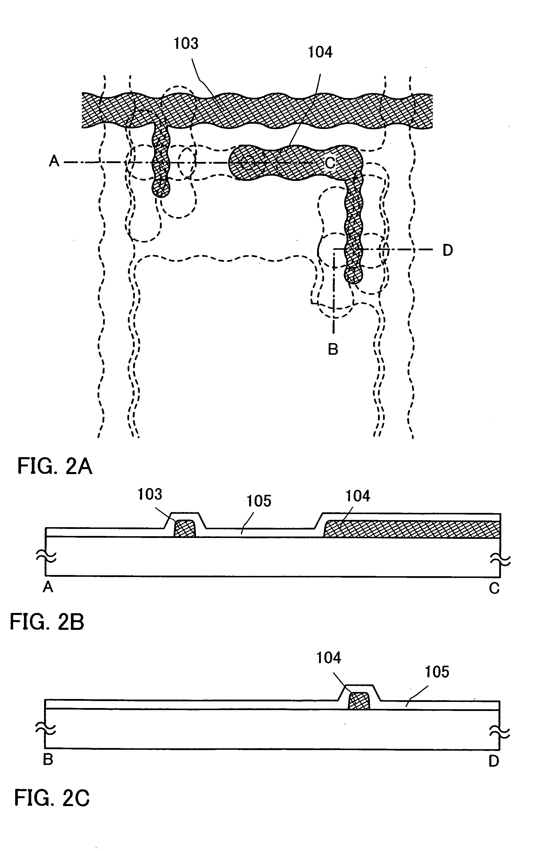
[0063] One feature of the present invention is that at least one or more of components required to manufacture a semiconductor device or a display device, such as a conductive layer for forming a wiring layer or an electrode, or a mask layer for forming a predetermined pattern, is / are formed by a method capable of selectively forming a pattern into a desired shape to manufacture a semiconductor device or a display device. In the present invention, a component (also referred to as a pattern) refers to a conductive layer such as a wiring layer, a gate electrode layer, a source electrode layer, or a drain electrode layer; a semiconductor layer; a mask layer; an insulating layer; or the like, which is included in a thin film transistor or a display device, and includes all components that are formed to have a predetermined shape. A droplet discharge (ejection) method (also referred to a...

embodiment mode 2

[0093]FIG. 26A is a top view showing a structure of a display panel using the present invention. A pixel portion 2701 in which pixels 2702 are arranged in matrix, a scanning line input terminal 2703, and a signal line input terminal 2704 are formed over a substrate 2700 having an insulating surface. The number of the pixels may be determined in accordance with various standards. In the case of XGA and RGB display, the number of the pixels may be 1024×768×3 (RGB). Similarly, in the case of UXGA and RGB display, the number of the pixels may be 1600×1200×3 (RGB), and in the case of a full-spec high vision and RGB display, it may be 1920×1080×3 (RGB).

[0094] The pixels 2702 are formed in matrix at intersections of scanning lines extended from the scanning line input terminal 2703 and signal lines extended from the signal line input terminal 2704. Each pixel 2702 is provided with a switching element and a pixel electrode connected thereto. A typical example of the switching element is a ...

embodiment mode 3

[0157] Embodiment Mode 3 of the present invention is described with reference to FIG. 13A to FIG. 19B. In more detail, a method of manufacturing a display device including a thin film transistor of a top gate planar structure using the present invention is described. FIGS. 13A, 14A, 15A, 16A, 17A, and 18A show a top view of a pixel portion of a display device. FIGS. 13B, 14B, 15B, 16B, 17B, and 18B show a sectional view taken along line E-F. FIG. 19A is also a top view of a display device, and FIG. 19B shows a sectional view taken along line O-W and line E-P in FIG. 19A. In addition, an example of a liquid crystal display device using a liquid crystal material for a display element is described. Repetitive explanations of the same portion and the portion having the same function are omitted.

[0158] A glass substrate made of barium borosilicate glass, alumino borosilicate glass, or the like; a quartz substrate; a metal substrate; or a plastic substrate which can withstand the process...


PUM


Abstract

Conductive layers having knots are adjacently formed with uniform distance therebetween. Droplets of the conductive layers are discharged to stagger centers of the droplets in a length direction of wirings so that the centers of the discharged droplets are not on the same line in a line width direction between the adjacent conductive layers. Since the centers of the droplets are staggered, parts of the conductive layers each having a widest line width (the widest width of knot) are not connected to each other, and the conductive layers can be formed adjacently with a shorter distance therebetween.

Description

BACKGROUND OF THE INVENTION [0001] 1. Field of the Invention [0002] The present invention relates to a semiconductor device, an electronic device, and a method of manufacturing a semiconductor device by using a printing method. [0003] 2. Description of the Related Art [0004] In a thin film transistor (hereinafter also referred to as TFT) and an electronic circuit using the thin film transistor, various thin films of a semiconductor, an insulator, a conductor, and the like are laminated over a substrate, and they are appropriately processed into predetermined patterns by a photolithography technique. The photolithography technique is a technique in which a pattern of a circuit or the like which is formed using a material that does not transmit light over a transparent flat plate which is referred to as a photomask is transferred to an intended substrate by utilizing light. The photolithography technique is widely used in a process of manufacturing a semiconductor integrated circuit a...

Claims


Application Information

Patent Timeline
IPC IPC(8): H01L23/52
CPCH01L21/02672H01L21/288H01L2924/0002H01L21/76838H01L27/12H01L27/3248H01L27/3276H01L51/0019H01L51/0022H01L51/0023H01L27/124H01L27/1285H01L27/1292H01L2924/00Y02P80/30H10K59/123H10K59/131H10K71/236H10K71/611H10K71/621
Inventor ISA, TOSHIYUKIFUJII, GENMORISUE, MASAFUMIKAWAMATA, IKUKO
Owner SEMICON ENERGY LAB CO LTD
Why Eureka
Try Eureka