Semiconductor device

a technology of electronic devices and semiconductors, applied in semiconductor lasers, instruments, optical elements, etc., can solve the problems of difficult to accurately dope a semiconductor with impurities, difficult to control pinch-off voltage, and difficult to give accurate carrier profiles through doping. achieve the effect of suppressing the local generation of piezo-charge, accurately controlling carrier density, and accurately controlling carrier density

Active Publication Date: 2006-08-10
PANASONIC CORP
View PDF6 Cites 20 Cited by
  • Summary
  • Abstract
  • Description
  • Claims
  • Application Information

AI Technical Summary

Benefits of technology

[0038] With the structural feature as described above, it is possible to surely suppress the local generation of piezo-charge caused by the stress to the active region. As a result, it is possible to realize the semiconductor device capable of controlling carrier density more accurately.
[0039] As has been described above, with the semiconductor device according to the present invention, it is possible to realize the semiconductor device which can accurately control carrier density without being affected by piezo-charge of extremely high density. Thus, it is possible to give an accurate c...

Problems solved by technology

Although the conventional AlGaN/GaN heterojunction on C-plane can realize a high sheet carrier density due to the polarization effect, it is difficult to effectively dope a semiconductor with impurities.
In other words, an amount of carriers generated by the polariz...

Method used


Image

  • Semiconductor device
  • Semiconductor device
  • Semiconductor device

Examples


first embodiment

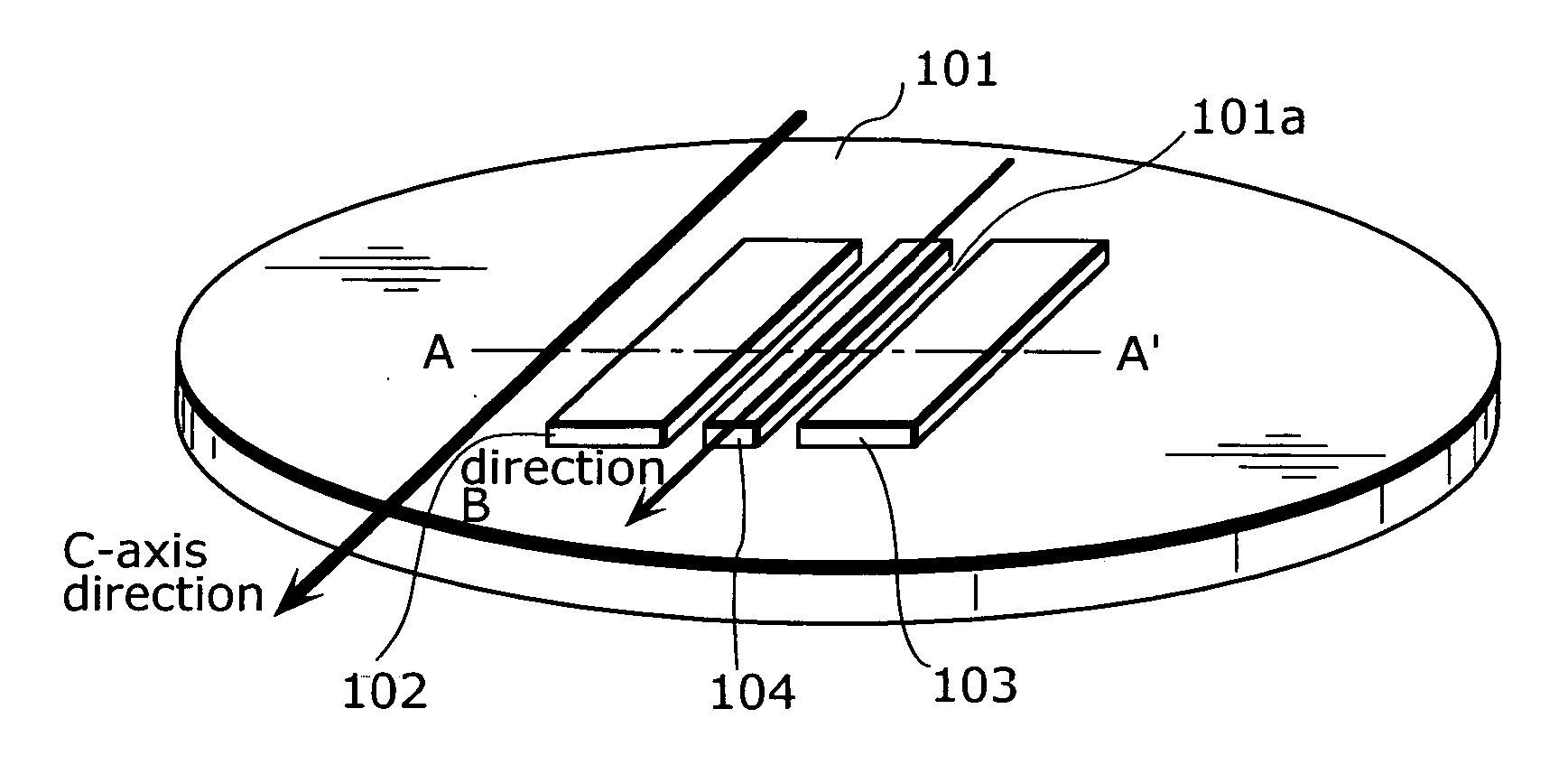
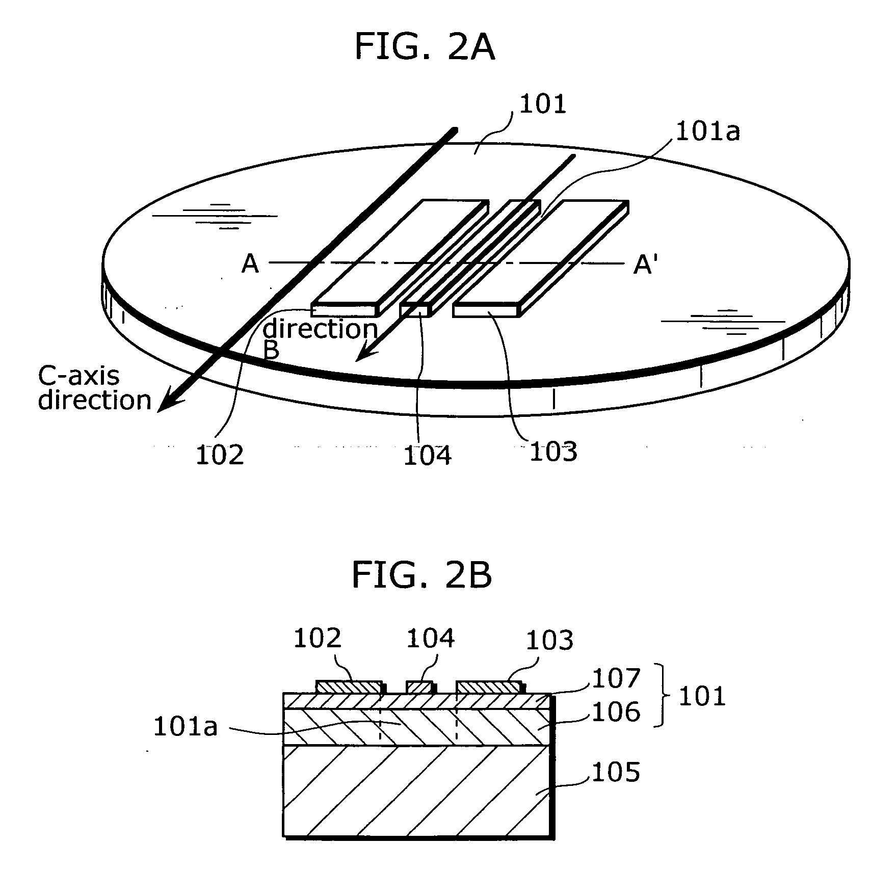
[0056]FIG. 2A is a diagonal view showing a Field-effect Transistor (FET) according to the first embodiment. FIG. 2B is a cross-sectional view of the FET at the A-A′ line shown in FIG. 2A. Note that FIG. 2A is a pattern diagram showing a part in which one FET is formed upon a wafer.

[0057] The FET according to the embodiment includes: a single crystal substrate 105; a semiconductor layer 101 which is made of hexagonal crystal with 6 mm symmetry, being In(x)Al(y)Ga(z)N (1-x-y-z) where 0≦x, y, z≦1, and x+y+z=1, and x, y and z are not simultaneously 0, and is formed on the main surface of the single crystal substrate 105 by epitaxial method; a source electrode 102; a drain electrode 103; and a gate electrode 104 which are formed on the main surface of the semiconductor layer 101.

[0058] The single crystal substrate 105 may be, for example, a sapphire substrate having R-plane as the main surface, or a silicon carbide (SiC) substrate having (11-20) plane as the main surface, or a GaN subs...

second embodiment

[0073]FIG. 6A is a diagonal view showing the FET according to the second embodiment, whereas FIG. 6B is a cross-sectional view of the FET at the line A-A′ in FIG. 6A. Note that FIG. 6A is a pattern diagram showing a part in which one FET is formed on a wafer. The same referential numbers are put for the same components as shown in FIG. 2, so that detailed description thereof is not repeated here.

[0074] The FET of the present embodiment differs from the FET according to the first embodiment in that the former has an active region whose length direction is vertical to the C-axis direction of hexagonal crystal, and is made up of a single crystal substrate 105 and a semiconductor layer 121 which is made of hexagonal crystal of 6 mm symmetry and is formed on the main surface of the single crystal substrate 105 based on an epitaxial growth method, a source electrode 102, as well as a drain electrode 103 and a gate electrode 104 which are formed on the main surface of the semiconductor la...

third embodiment

[0080]FIG. 7 is a diagonal view showing a structure of the semiconductor laser device according to the third embodiment.

[0081] The semiconductor laser device according to the present embodiment includes: an n-type GaN substrate 146 having (11-20) plane as the main surface; a semiconductor layer 141 which is made of In(x)Al(y)Ga(z)N (1-x-y-z), where 0≦x, y, z>1, and x+y+z=1, and x, y and z do not indicate 0 at the same time of hexagonal crystal with 6 mm symmetry, and which is formed on the main surface of the n-type GaN substrate 146 based on epitaxial growth method; an n-type electrode 147 which is formed on the rear surface of the n-type GaN substrate 146 and is made of, for instance, Ti, Au and the like; and a p-type electrode 148 which is formed on the main surface of the semiconductor layer 141 and has a multi-layered structure made of, for example, Ni, Pt and Au. Note that the size of one semiconductor laser device within the surface of the substrate is 500 μm×300 μm (500 μm ...


PUM


Abstract

A semiconductor device, which can accurately control carrier density, includes: a single crystal substrate; a semiconductor layer which is made of hexagonal crystal with 6 mm symmetry and is formed on the single crystal substrate; a source electrode, a drain electrode and a gate electrode which are formed on the semiconductor layer, where the main surfaces of a GaN layer and an AlGaN layer constituting the semiconductor layer respectively include C-axis of the hexagonal crystal, and a length direction of a channel region in the semiconductor layer is parallel to the C-axis of the hexagonal crystal.

Description

BACKGROUND OF THE INVENTION [0001] (1) Field of the Invention [0002] The present invention relates to a nitride electronic device intended for power switching as represented by an inverter used for an electric vehicle and a home electric appliance, and also relates to a nitride optical device as represented by a blue / white light-emitting diode (LED) and a laser device. [0003] (2) Description of the Related Art [0004] Recently, a nitride semiconductor has been under intense research and development as a material for high-output power devices or blue light-emitting devices, to the extent that an optical device using a nitride semiconductor, in particular, has already been introduced into the market. [0005] A Modulation Doped Field-effect Transistor (MODFET) applying an aluminum gallium nitride (AlGaN) / gallium nitride (GaN) heterojunction is studied as an electronic device. The most significant difference between such MODFET and a gallium arsenide (GaAs) MODFET is that the former MODFE...

Claims


Application Information

Patent Timeline
IPC IPC(8): H01L33/00H01L33/16H01L33/20
CPCB82Y20/00H01L29/045H01L29/2003H01L29/7787H01L33/16H01L33/20H01S5/2201H01S5/34333G02B1/02
Inventor ISHIDA, HIDETOSHI
Owner PANASONIC CORP
Why Eureka
Try Eureka