Semiconductor device and fabrication method thereof

Inactive Publication Date: 2006-08-10
FUJITSU MICROELECTRONICS LTD
View PDF12 Cites 38 Cited by
  • Summary
  • Abstract
  • Description
  • Claims
  • Application Information

AI Technical Summary

Benefits of technology

[0031] Oxygen-free RF plasma etching allows the altered layer to be removed efficiently, while preventing s

Problems solved by technology

However, as the bump pitch becomes narrower, it becomes more dif

Method used


Image

  • Semiconductor device and fabrication method thereof
  • Semiconductor device and fabrication method thereof
  • Semiconductor device and fabrication method thereof

Examples


first embodiment

[0043]FIG. 3A through FIG. 3F illustrate a semiconductor device fabrication process according to the invention.

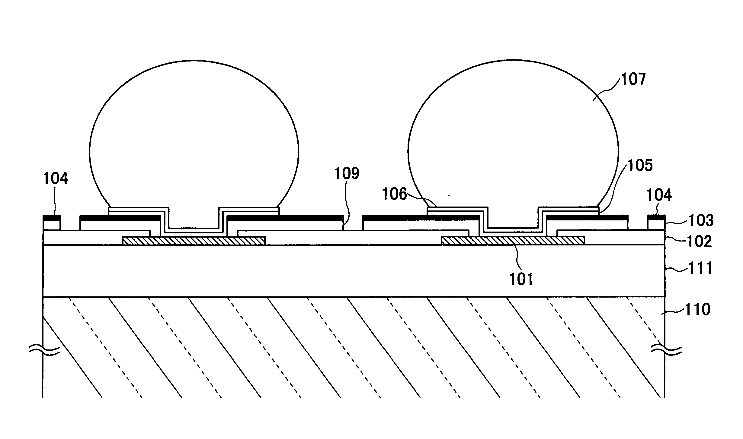
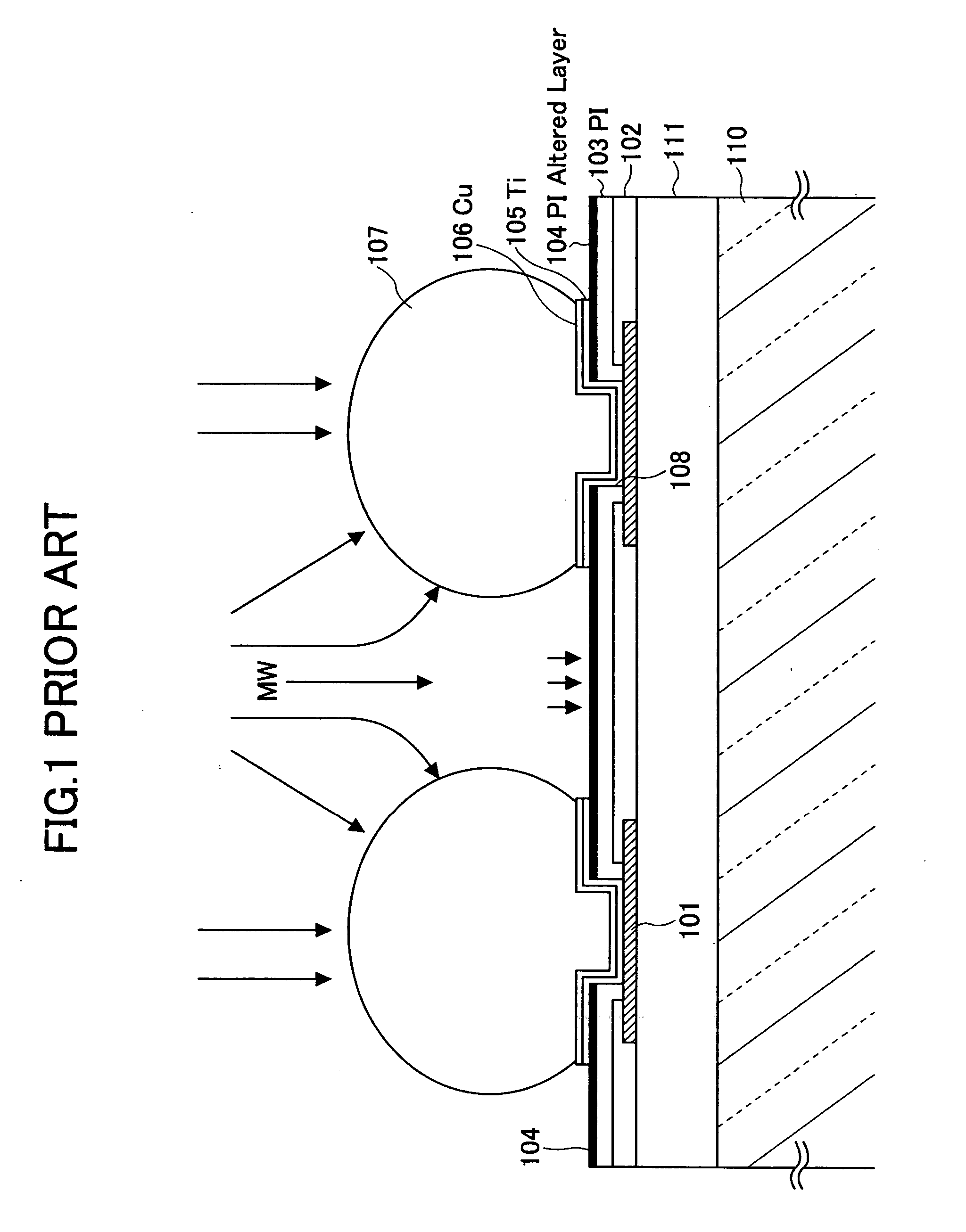
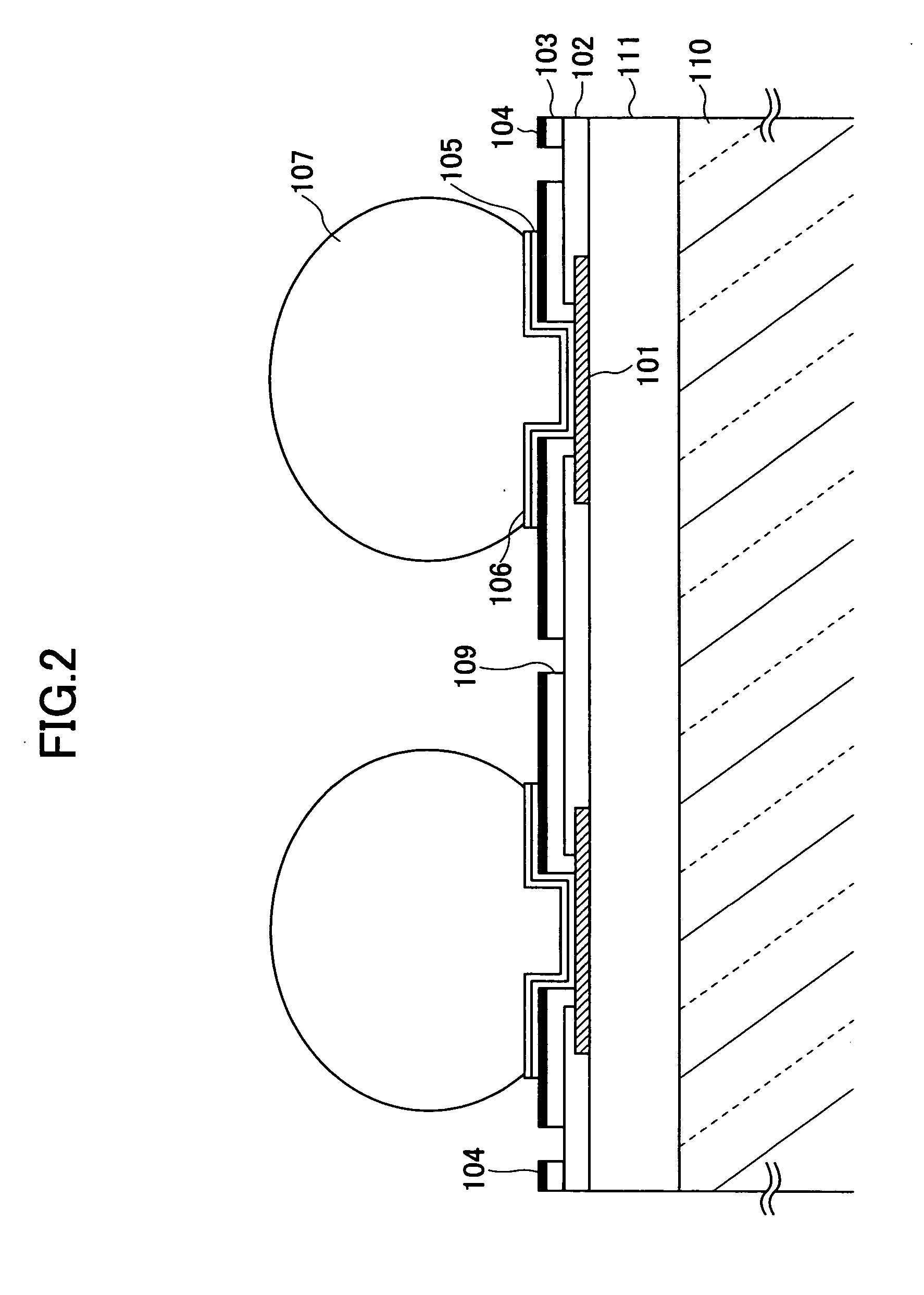
[0044] First, as illustrated in FIG. 3A, aluminum (Al) pad 11 is formed at a prescribed position on a semiconductor wafer 20 in which internal circuits (not shown) are formed and covered with dielectric layers. The pad 11 provides electric connection with the internal circuit. The pad 11 and the entire surface of the semiconductor wafer 20 are covered with a passivation film (cover film) 12. An opening is formed in the passivation film 12 so as to expose the surface of the Al pad 11. Then, a photosensitive or nonphotosensitive polyimide overcoat (organic coat) 13 is formed over the exposed Al pad 11 and the passivation film 12. The thickness of the polyimide film 13 is 1 μm to 20 μm, depending on the design. A prescribed position of the polyimide film 13 is etched to form an opening 23 so as to expose the Al pad 11. Then, radio-frequency RF etching is performed as pretreatm...

second embodiment

[0068] In the second embodiment, a wet process is carried out, prior to the dry process, to remove the titanium (Ti) particles implanted in the altered layer 14. This arrangement allows existing microwave (MW) ashers to be used for the removal of the altered layer. However, it is desired to employ RF etching even when the dry process is combined with the wet process, taking into account the overetch depth and the surface degradation (such as tarnish) of the polyimide layer 13.

[0069]FIG. 6A though FIG. 6C illustrate a modification of the semiconductor device fabrication process of the second embodiment. The step shown in FIG. 6A follows the step shown in FIG. SD.

[0070] In FIG. 6A, reflow treatment is carried out after the unnecessary portions of the Cu film 16 and the Ti film 15 have been removed, thereby forming a bump or protruding electrode 22. After the reflow, light wet etching is performed using 0.5% hydrofluoric (HF) acid to remove the titanium (Ti) particles implanted into t...

third embodiment

[0087] In the third embodiment, the altered layer 14 is removed following the under bump metallization, and therefore an existing microwave (MW) asher can be utilized. By providing the gold (Au) thin film on the top of the UBM, certain types of oxygen-mixed gas may be used for the microwave ashing. However, using oxygen-free etching gas is preferable from the viewpoint of preventing oxidation on the side edge of the nickel (Ni) plating layer 18.

[0088]FIG. 9A and FIG. 9B illustrate a semiconductor device fabrication process according to the fourth embodiment of the invention. In the fourth embodiment, removal of an altered layer is applied to the formation of a copper (Cu) interconnection on a redistribution layer (RDL).

[0089]FIG. 9A includes a cross-sectional view and a top view of a redistribution layer in which a copper (Cu) interconnection 31 is formed with the altered layer 14 remaining on the wafer.

[0090] Prior to forming the copper (Cu) interconnection 31, an aluminum (Al) p...


PUM


Abstract

A semiconductor device fabrication method comprises the steps of: (a) forming a pad electrode on the semiconductor device; (b) coating the surface of the semiconductor device with an organic dielectric film so as to expose the center portion of the pad electrode; (c) treating the exposed surface of the pad electrode by dry etching; and (d) removing an altered layer produced in the organic dielectric film due to the dry etching for the surface treatment, using an oxygen-free dry process.

Description

BACKGROUND OF THE INVENTION [0001] 1. Field of the Invention [0002] The present invention generally relates to a semiconductor device with bump electrodes (or protruding electrodes) and a fabrication method thereof, and more particularly, to removal of an altered layer generated in the surface area of an organic dielectric due a dry etching process for native oxide removal from a metal surface (such as a metal pad), in order to prevent surface leakage. [0003] 2. Description of the Related Art [0004] Providing protruding electrodes or bump electrodes on a semiconductor device, such as an IC chip, has become mainstream, which technique allows the chip to be mounted directly on a substrate. In recent years and continuing, the bump pitch becomes narrower and narrower along with the miniaturization of the semiconductor devices and the packages. [0005] A bump is formed on a pad electrode to provide electric connection with internal electrodes. In general, the surface of a semiconductor de...

Claims


Application Information

Patent Timeline
IPC IPC(8): H01L23/58
CPCH01L21/0206H01L24/11H01L2224/1147H01L2224/13099H01L2924/01002H01L2924/0101H01L2924/01013H01L2924/01018H01L2924/01022H01L2924/01029H01L2924/01033H01L2924/01047H01L2924/01074H01L2924/01075H01L2924/01078H01L2924/01079H01L2924/01082H01L2924/14H01L24/13H01L2924/01005H01L2924/01006H01L2924/01023H01L2924/01072H01L2924/014H01L2224/131H01L2224/13111H01L2924/00014H01L2924/0001H01L2924/351H01L2224/05027H01L2224/05022H01L2224/05001H01L2224/05572H01L2224/05124H01L2224/05147H01L2224/05155H01L2224/05166H01L2224/05644H01L2224/05655H01L2224/02375H01L2224/05548H01L2224/06152H01L2224/06154H01L24/06H01L24/05H01L24/03H01L2924/00
Inventor MURATA, KOICHIIKUMO, MASAMITSUWATANABE, EIJI
Owner FUJITSU MICROELECTRONICS LTD
Why Eureka
Try Eureka