Low temperature deposition of silicon oxides and oxynitrides

Inactive Publication Date: 2006-08-10
AVIZA TECHNOLOGY INC +1
View PDF82 Cites 53 Cited by
  • Summary
  • Abstract
  • Description
  • Claims
  • Application Information

AI Technical Summary

Benefits of technology

[0008] Low temperature (i.e., less than about 450° C.) deposition processes are provided for depositing silicon oxide and silicon oxynitride layers for spacer and pre-metal dielectric applications. The processes, which can be either CVD and ALD proce

Problems solved by technology

However, present techniques, including present CVD techniques, for applying such films become less and less suitable as line width dimensions in integrated circuitry (IC) continue to scale down.
However, such CVD processes generally require temperatures above 600° C.—although bis(tertiary-butylamino)silane (BTBAS) and diethylsilane (Et2SiH2) react with oxygen gas (O2) at 400° C. Such high temperatures result in oxidation of contact metals such as tungsten, thereby increasing line resistance.
In addition, such high temperatures result in catalytic reaction of metals to form undesirable whiskers such as tu

Method used


Image

  • Low temperature deposition of silicon oxides and oxynitrides
  • Low temperature deposition of silicon oxides and oxynitrides
  • Low temperature deposition of silicon oxides and oxynitrides

Examples


Embodiment Construction

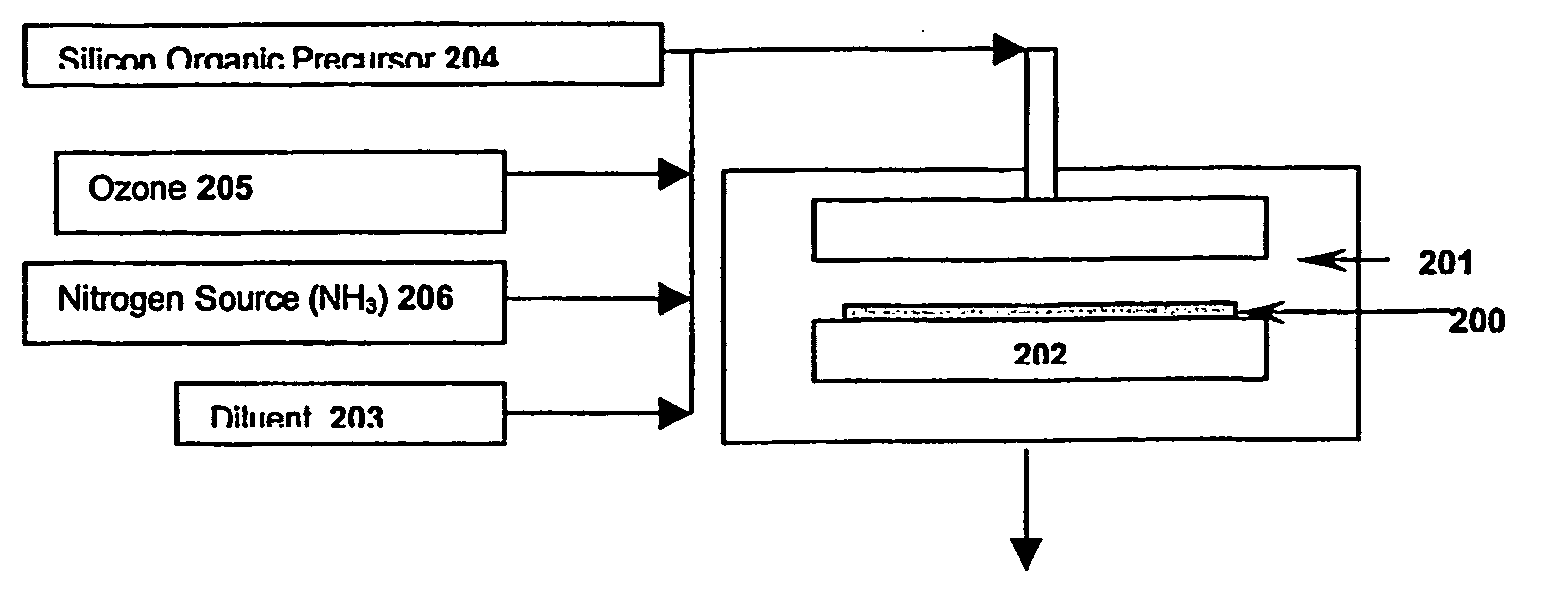
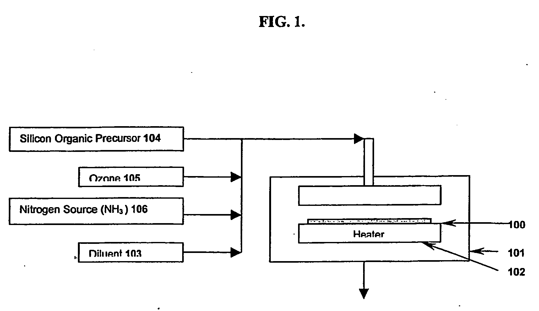
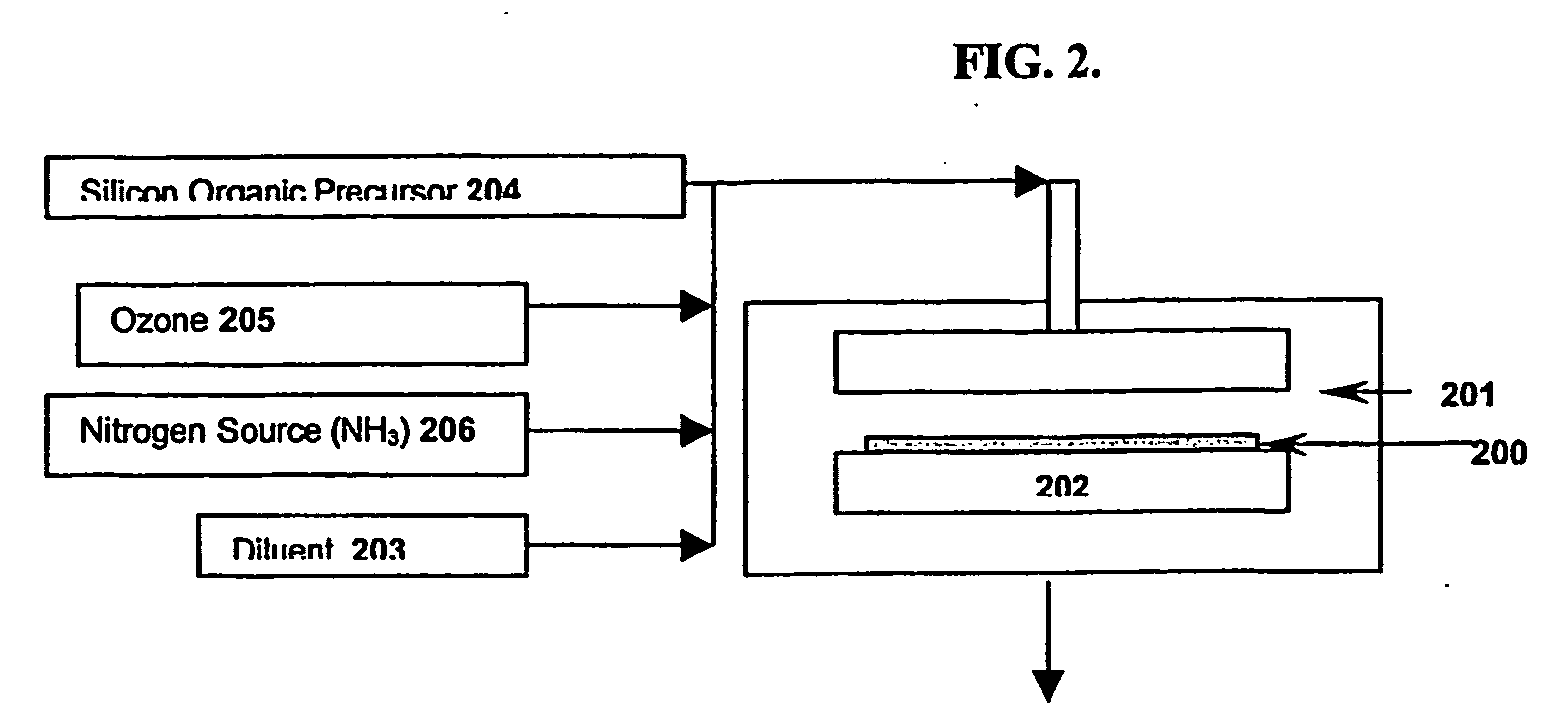
[0016] The present invention provides CVD and ALD methods of depositing silicon oxide and silicon oxynitride films on a substrate at low temperatures, i.e., below about 450° C., while simultaneously maintaining good step coverage characteristics. The methods of the invention utilize metal silicon organic precursors in combination with ozone. The deposition methods of the present invention can be used in depositing both high-k and low-k dielectrics.

[0017] The substrate to be coated can be any material with a metallic or hydrophilic surface which is stable at the processing temperatures employed. Suitable materials will be readily evident to those of ordinary skill in the art. Suitable substrates include silicon, ceramics, metals, plastics, glass and organic polymers. Preferred substrates include silicon, tungsten and aluminum. The substrate may be pretreated to instill, remove, or standardize the chemical makeup and / or properties of the substrate's surface. The choice of substrate i...


PUM

PropertyMeasurementUnit
Temperatureaaaaaaaaaa

Abstract

The present invention relates to low temperature (i.e., less than about 450° C.) chemical vapor deposition (CVD) and low temperature atomic layer deposition (ALD) processes for forming silicon oxide and/or silicon oxynitride derived from silicon organic precursors and ozone. The processes of the invention provide good step coverage. The invention can be utilized to deposit both high-k and low-k dielectrics.

Description

CROSS-REFERENCE TO RELATED APPLICATIONS [0001] This application is related to, and claims priority to, U.S. Provisional Patent Application No. 60 / 404,363, entitled Low Temperature Deposition of Silicon Oxides and Oxynitrides, filed Aug. 18, 2002.FIELD OF THE INVENTION [0002] The present invention relates to the field of semiconductors. More specifically, the present invention relates to low temperature chemical vapor deposition (CVD) and low temperature atomic layer deposition (ALD) processes for forming silicon oxide and / or silicon oxynitride from silicon organic precursors and ozone. BACKGROUND OF THE INVENTION [0003] CVD is a known deposition process. In CVD, two or more reactant gases are mixed together in a deposition chamber where the gases react in the gas phase and either deposit a film onto a substrate's surface or react directly on the substrate's surface. Deposition by CVD occurs for a specified length of time, based on the desired thickness of the deposited film. Since t...

Claims


Application Information

Patent Timeline
IPC IPC(8): H01L21/31H01L21/205C23C16/30C23C16/40C23C16/44C23C16/455H01L21/314H01L21/316H01L21/318
CPCC23C16/308C23C16/401C23C16/45525C23C16/45531C23C16/45553H01L21/0214H01L21/31612H01L21/02219H01L21/02271H01L21/0228H01L21/3141H01L21/3145H01L21/02164
Inventor SENZAKI, YOSHIHIDELEE, SANG-INLEE, SANG-KYOO
Owner AVIZA TECHNOLOGY INC
Why Eureka
Try Eureka