Magnetoresistance device including layered ferromagnetic structure, and method of manufacturing the same
a ferromagnetic structure and magnetoresistance technology, applied in the field of magnetoresistance devices, can solve the problems of inability to increase the volume of the free magnetic layer undetectedly, and inability to reverse the magnetization of the free magnetic layer. achieve the effect of great exchange coupling
- Summary
- Abstract
- Description
- Claims
- Application Information
AI Technical Summary
Benefits of technology
Problems solved by technology
Method used
Image
Examples
first embodiment
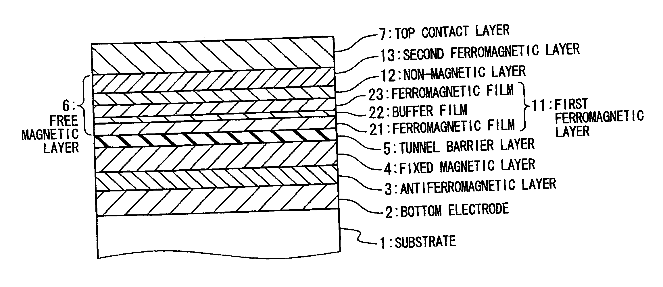
[0131]FIG. 5A is a sectional view showing an exemplary structure of MRAM memory cells in a first embodiment of the present invention. An MRAM is composed of a substrate 1, a bottom electrode 2 formed on the substrate 1, an antiferromagnetic layer 3 formed of antiferromagnetic material, a fixed magnetic layer 4, a tunnel barrier layer 5, a free magnetic layer 6 and a top contact layer 7. The antiferromagnetic layer 3 fixes the magnetization of the fixed magnetic layer 4 by exchange interaction therebetween. The fixed magnetic layer 4 is composed of a single ferromagnetic layer or an SAF, and the magnetizations) thereof is fixed by the antiferromagnetic layer 3.
[0132] The tunnel barrier layer 5 is composed of a very thin non-magnetic insulative layer. In this embodiment, many materials may be used for the tunnel barrier layer 5. In an aspect of the crystalline structure, the tunnel barrier layer 5 may be formed of amorphous or crystalline material. Specifically, the tunnel barrier la...
second embodiment
[0159] One issue of the structure of the free magnetic layer 6 shown in FIG. 5A is the difference in the characteristics between the first and second ferromagnetic layers 11 and 13 resulting from the structure difference therebetween. The large difference in the characteristics between the first and second ferromagnetic layers 11 and 13, especially, the large difference in the crystal magnetic anisotropy and the magnetization-and-thickness product is undesirable for implementing the toggle writing.
[0160] In a second embodiment, a technique is provided for reducing the difference in the characteristics between the first and second ferromagnetic layers 11 and 13. Specifically, in the second embodiment, as shown in FIG. 8, the second ferromagnetic layer 13 is composed of a plurality of ferromagnetic films 26, 28, and a buffer film 27 placed therebetween. It should be noted that the structure of the first ferromagnetic layer 11 may be any of the structures shown in FIGS. 5A, 5B, 7A and...
third embodiment
[0169] In a third embodiment, a technique is provided in which three or more ferromagnetic layers are incorporated within the free magnetic layer 6. The increase in the number of the ferromagnetic layers within free magnetic layer 6 is effective for avoiding undesirable magnetization reversal of the free magnetic layer 6 due to the thermal activation, because it increases the total volume of the ferromagnetic layers within the free magnetic layer 6. As described later, it should be noted that the term “ferromagnetic layer” described here means to include the layer in which adjacent two ferromagnetic films are antiferromagnetically coupled.
[0170]FIG. 12 shows an exemplary MRAM structure in which the free magnetic layer 6 is composed of the three ferromagnetic layers: a first ferromagnetic layer 11, a second ferromagnetic layer 13 and a third ferromagnetic layer 15. A non-magnetic layer 12 is inserted between the first and second ferromagnetic layers 11 and 13, and another non-magnet...
PUM
 Abstract
Description
Claims
Application Information


