Solar cell using carbon nanotubes and process for producing the same

a carbon nanotube and solar cell technology, applied in the field of solar cells, can solve the problems of inability to be environmentally thoughtful, process uses toxic raw material gases, and solar cell using organic semiconductors have not yet been put into practical application, and achieve the effect of high photoelectric conversion efficiency and easy production

Inactive Publication Date: 2006-08-24
FUJIFILM BUSINESS INNOVATION CORP
View PDF12 Cites 80 Cited by
  • Summary
  • Abstract
  • Description
  • Claims
  • Application Information

AI Technical Summary

Benefits of technology

[0009] The invention is to provide such a solar cell of a pn junction type or a pin junction type that is easily produced and has a high photoelectric conversion efficiency by using an organic semiconductor containing carbon nanotubes, and to provide a process for producing the same.

Problems solved by technology

However, the production process of the solar cell using an inorganic thin film semiconductor requires a special equipment to raise the production cost of the solar cell, and furthermore, the process uses toxic raw material gases.
Therefore, the process cannot be environmentally thoughtful.
However, a solar cell using an organic semiconductor has not yet been put into practical application because of the low photoelectric conversion efficiency thereof.
The reason why the solar cell using an organic semiconductor has a low photoelectric conversion efficiency includes the low photocarrier forming capability of the organic semiconductor, the narrow photocarrier forming region around the junction as compared to an inorganic semiconductor, and the low capability of transporting the carriers thus formed.
As a result, only a small electric current is formed to provide low photoelectric conversion efficiency.

Method used


Image

  • Solar cell using carbon nanotubes and process for producing the same
  • Solar cell using carbon nanotubes and process for producing the same
  • Solar cell using carbon nanotubes and process for producing the same

Examples


example 1

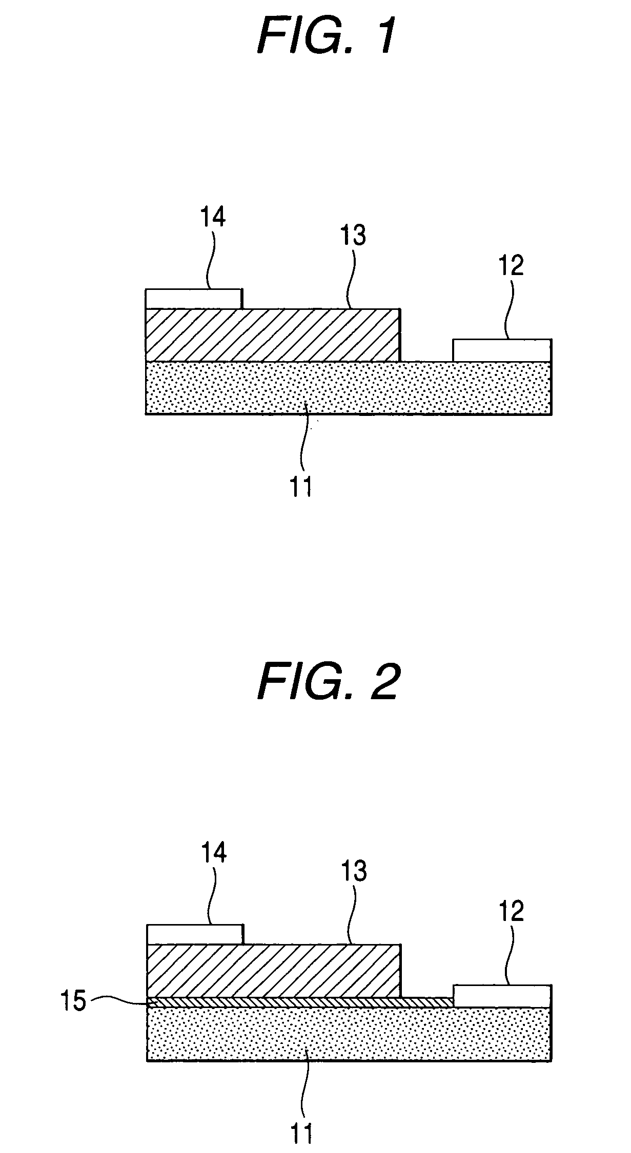
[0228] A solar cell of a pin junction having a constitution shown in FIG. 2 is produced by using a carbon nanotube structure as a p-type semiconductor substance.

Production of Carbon Nanotube Structure Film

[0229] A carbon nanotube structure film is produced in the following manner.

[0230] 30 mg of single wall carbon nanotube powder (purity: 90%, average diameter 1.1 nm, length: 0.5 to 100 μm, produced by Sigma Aldrich, Inc.) is added to 20 mL of concentrated nitric acid (60% by mass aqueous solution, produced by Kanto Kagaku Co., Ltd.), and the mixture is refluxed at 120° C. for 1.5 hours to synthesize carbon nanotube carboxylic acid.

[0231] The temperature of the solution is lowered to room temperature, and the solution is subjected to centrifugal separation at 5,000 rpm for 15 minutes to separate a precipitate from a supernatant fluid. The precipitate thus recovered is dispersed in 10 mL of pure water and then again subjected to centrifugal separation at 5,000 rpm for 15 minutes...

example 2

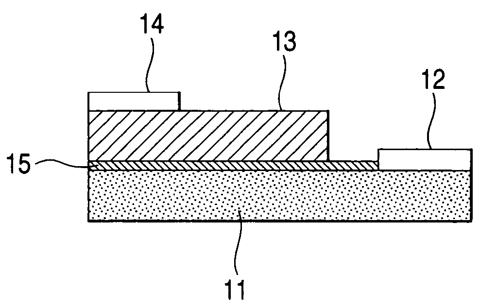
[0246] A solar cell of a pn junction having a constitution shown in FIG. 1 is produced by using a carbon nanotube structure as a p-type semiconductor substance.

[0247] On the same n-type silicon (n-Si) substrate (thickness: 625 μm, thermal oxidation film of 10 nm, 8 to 12 Ωcm, mirror finished, dimension: 10 mm×15 mm) as in Example 1, an electrode 12 (dimension: 5 mm square, 10 nm of titanium and 100 nm of gold) is formed in the same manner as in Example 1. In order to form a pn junction, the substrate is immersed in buffered hydrofluoric acid (HF: 20% by volume, NH4F: 21% by volume, H2O: 57% by volume) for 60 seconds to remove a thermal oxidation film on the surface of the n-type silicon substrate.

[0248] About 20 μL of a precursor coating composition containing SWNT each having a functional group, which is prepared in the same manner as in Example 1, is coated on the surface of the n-type silicon substrate having no thermal oxidation film to an area of 5 mm×10 mm and then heated to...


PUM


Abstract

A solar cell includes a p-type semiconductor substance, and an n-type semiconductor substance. The p-type semiconductor substance and the n-type semiconductor substance form a pn junction or a pin junction, and the p-type semiconductor substance or the n-type semiconductor substance includes a structure film having a plurality of carbon nanotubes electrically connected to each other.

Description

BACKGROUND OF THE INVENTION [0001] 1. Field of the Invention [0002] The present invention relates to a solar cell, and more particularly, it relates to a solar cell utilizing an internal electric field formed with a pn junction or a pin junction, and a process for producing the same. [0003] 2. Description of the Related Art [0004] Studies for utilizing the solar energy as environmentally thoughtful energy have been earnestly made. In particular, such a solid state device has been earnestly studied that converts the solar energy directly to electric energy using an inorganic semiconductor, owing to the high photoelectric conversion efficiency thereof, and solar cells utilizing single crystal, polycrystalline or amorphous silicon have been put into practical use. The solar cell utilizing an inorganic semiconductor attains a photoelectric conversion efficiency (energy conversion efficiency, i.e., a ratio of generated electric energy to incident light energy) reaching, for example, abou...

Claims


Application Information

Patent Timeline
Patent Type & Authority Applications(United States)
IPC IPC(8): H01L31/105B82Y20/00H01L51/42H01L51/44
CPCB82Y10/00B82Y30/00H01L31/0256H01L31/06H01L51/0012H01L51/0049H01L51/4213Y02E10/549Y02E10/547Y02P70/50H10K71/191H10K85/225H10K30/10
Inventor SHIMOTANI, KEIMANABE, CHIKARAMORIKAWA, TAKASHI
Owner FUJIFILM BUSINESS INNOVATION CORP
Why Eureka
Try Eureka