
Brightness-enhanced multilayer optical film with low reflectivity for display and organic light emitting diode display using the same

a multi-layer optical film and light-emitting diode technology, applied in the direction of discharge tube luminescnet screens, other domestic articles, organic semiconductor devices, etc., can solve the problems of low light-emitting device light-emitting device efficiency drop, light-emitting device fabricated through difficult layer formation at increased costs compared to conventional fabrication of light-emitting devices, etc., to achieve low reflectivity and high light-emitting efficiency , the effect of high-

Active Publication Date: 2006-08-24
CHEIL IND INC
View PDF5 Cites 48 Cited by
  • Summary
  • Abstract
  • Description
  • Claims
  • Application Information

AI Technical Summary

Benefits of technology

[0012] It is an object of the present invention to provide a brightness-enhancing multilayer optical film with low reflectivity for an OLED display and an OLED display using the optical film.

Problems solved by technology

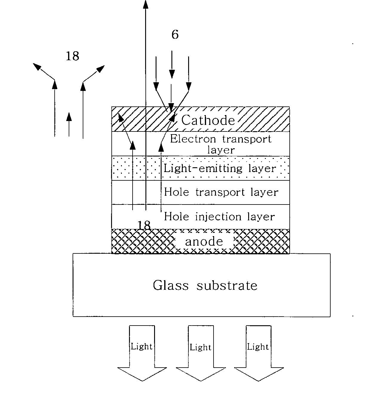
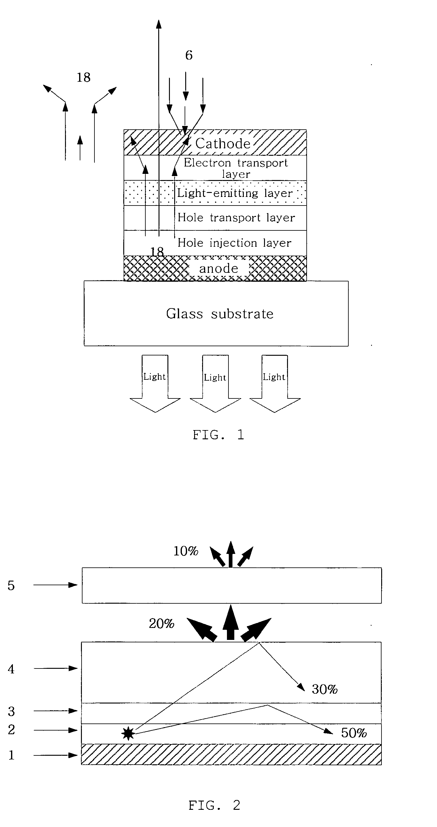
This internal reflection of the external light from the cathode becomes a cause of deterioration in the contrast of an OLED display.
As shown in FIG. 2, main causes of brightness degradation in a conventional OLED display are total reflection effects, resulting from different refractive indices of respective layers constituting a light-emitting device, and a polarization phenomenon, resulting from the use of a circular polarizing plate.
The light-absorbing material contained or injected in this manner reduces the amount of external light entering the light-emitting device can be reduced, but absorbs a portion of light generated from the light-emitting layer, dropping the light-output efficiency of the light-emitting device.
As a result, the light-emitting device shows poor brightness properties.
Further, since mixing the light-absorbing material with materials constituting the electron transport layer and the electron injection layer or formation of an additional light-absorbing layer is a process changing the layer structure and the layer-constituent materials of the light-emitting device, the light-emitting device is fabricated through difficult layer formation in low yield at increased costs as compared to conventional fabrication of light-emitting devices.

Method used


Image

  • Brightness-enhanced multilayer optical film with low reflectivity for display and organic light emitting diode display using the same
  • Brightness-enhanced multilayer optical film with low reflectivity for display and organic light emitting diode display using the same
  • Brightness-enhanced multilayer optical film with low reflectivity for display and organic light emitting diode display using the same

Examples


example 1

[0077] A 100 μm-thick polyethylene terephthalate (PET) film was used as a transparent substrate. A coating solution for a light diffusion layer was prepared by the following procedure. First, 200 parts by weight of light-diffusing particles having an average diameter of 5 μm were sufficiently stirred and dispersed in a mixed solvent containing 300 parts by weight of isopropyl alcohol (IPA), 300 parts by weight of methyl ethyl ketone (MEK), 200 parts by weight of toluene and 100 parts by weight of cyclopentanone to obtain a dispersion of the light-diffusing particles. 100 parts by weight (solid content) of a heat-curable acrylic resin (Aekyung Chemical, Korea) was mixed with the dispersion, and then stirred for 3 hours to obtain a particle-dispersed resinous solution. One hour before formation of a light diffusion layer, 25 parts by weight of an isocyanate curing agent (Aekyung Chemical, Korea) was added to the resinous solution to prepare a coating solution for a light diffusion lay...

example 2

[0078] A multilayer optical film was produced in the same manner as in Example 1, except that the light-absorbing particles were used in an amount of 150 parts by weight to form a light-absorbing layer on the light diffusion layer.

example 3

[0079] An OLED display was manufactured by laminating the optical film produced in Example 1 or 2 in such a manner that an adhesive layer positioned opposite to the light-absorbing layer of the optical film was attached on top of a transparent substrate (indium-titanium oxide (ITO) glass) of a 14.1-inch OLED display (Samsung Electronics, Korea). The brightness of white light was measured at 500 1x.


PUM


Abstract

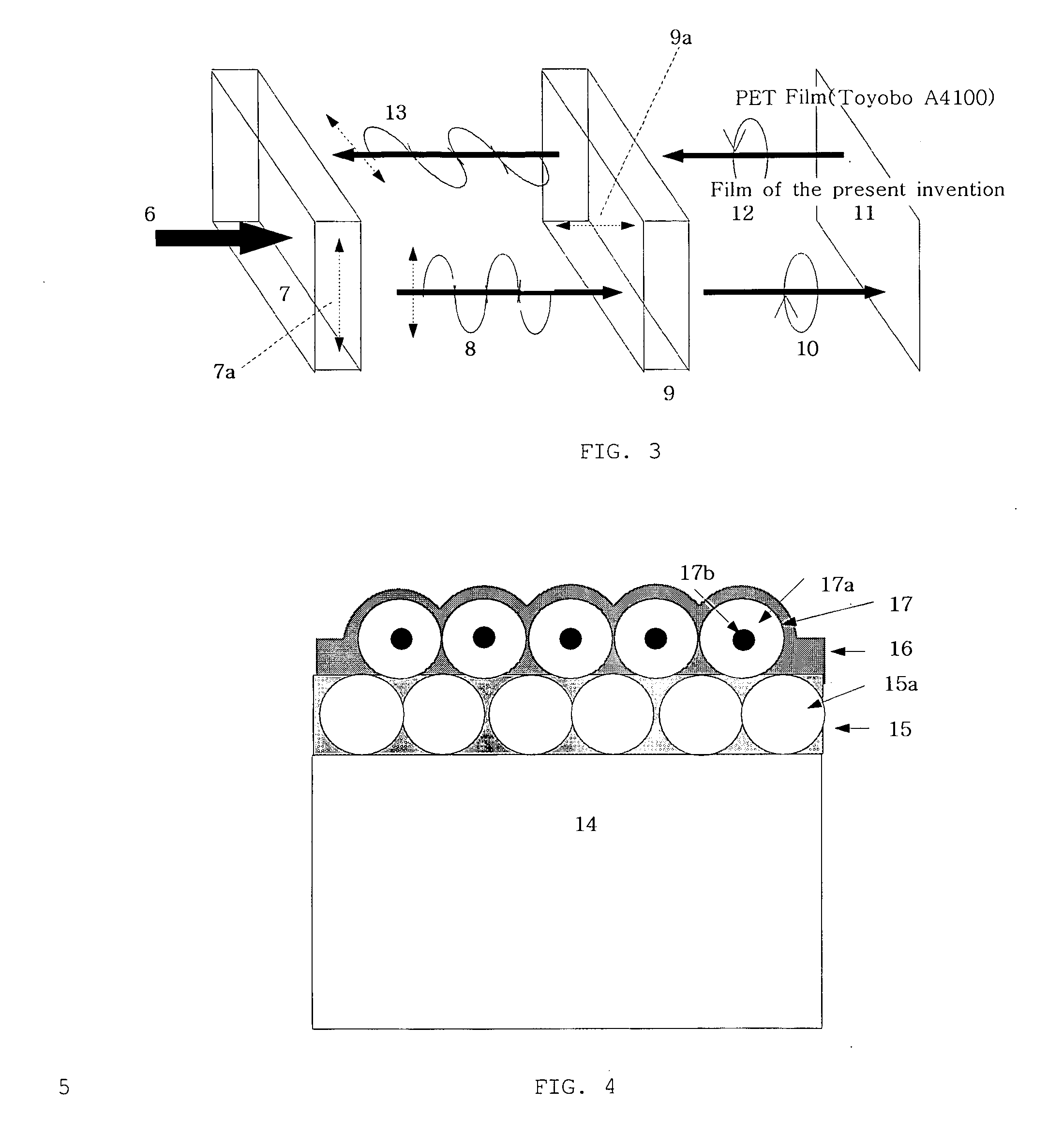
Disclosed herein is a low-reflectivity, brightness-enhancing multilayer optical film for enhancing the brightness of an organic light emission diode (OLED) display and imparting anti-reflection performance to the display. The multilayer optical film comprises a transparent substrate, a light diffusion layer formed on the transparent substrate by wet coating and a light-absorbing layer formed on the light diffusion layer by wet coating wherein the substrate has a thickness of 10˜300 μm, the light diffusion layer contains a resin and spherical particles, and the light-absorbing layer contains 50˜500 parts by weight of core-shell structured light-absorbing particles composed of a light-absorbing agent as a material for the core and a transparent resin as a material for the shell. Further disclosed is an organic light emitting diode (OLED) display using the multilayer optical film.

Description

[0001] This non-provisional application claims priority under 35 U.S.C. §119(a) on Korean Patent Application No. 2005-14862 filed on Feb. 23, 2005, which is herein incorporated by reference. BACKGROUND OF THE INVENTION [0002] 1. Field of the Invention [0003] The present invention relates to a low-reflectivity, brightness-enhancing multilayer optical film that can be used in a display, and more particularly to a brightness-enhancing multilayer optical film comprising a transparent substrate, a light diffusion layer formed on the transparent substrate by wet coating and a light-absorbing layer formed on the light diffusion layer by wet coating wherein the substrate has a thickness of 10˜300 μm, the light diffusion layer contains a resin and spherical particles, and the light-absorbing layer contains 50˜500 parts by weight of core-shell structured light-absorbing particles composed of a light-absorbing agent as a material for the core and a transparent resin as a material for the shell...

Claims


Application Information

Patent Timeline
Patent Type & Authority Applications(United States)
IPC IPC(8): H05B33/00
CPCH01L51/5281H01L51/5284H01L2251/558H10K2102/351H10K59/8791H10K59/8792A47G29/087E03C1/06H10K50/86H10K50/865
Inventor LIM, SANG KYOOLIM, TAE KYUNGSEO, HWI MINSONG, LEE HWA
Owner CHEIL IND INC
Learn More