P-n heterojuction structure of zinc oxide-based nanorod and semiconductor thin film, preparation thereof, and nano-device comprising same

Active Publication Date: 2006-08-24
LG DISPLAY CO LTD
View PDF37 Cites 61 Cited by
  • Summary
  • Abstract
  • Description
  • Claims
  • Application Information

AI Technical Summary

Benefits of technology

[0005] Accordingly, it is a primary object of the present invention to provide a novel heterojunction structure formed by way of using n-ZnO in the form of a nanorod and a p-type se

Problems solved by technology

However, the development of a p-n heterojunction structure of zinc ox

Method used


Image

  • P-n heterojuction structure of zinc oxide-based nanorod and semiconductor thin film, preparation thereof, and nano-device comprising same
  • P-n heterojuction structure of zinc oxide-based nanorod and semiconductor thin film, preparation thereof, and nano-device comprising same
  • P-n heterojuction structure of zinc oxide-based nanorod and semiconductor thin film, preparation thereof, and nano-device comprising same

Examples


example 1

The Growth of ZnO Nanorods on a P-Type GaN Thin Film

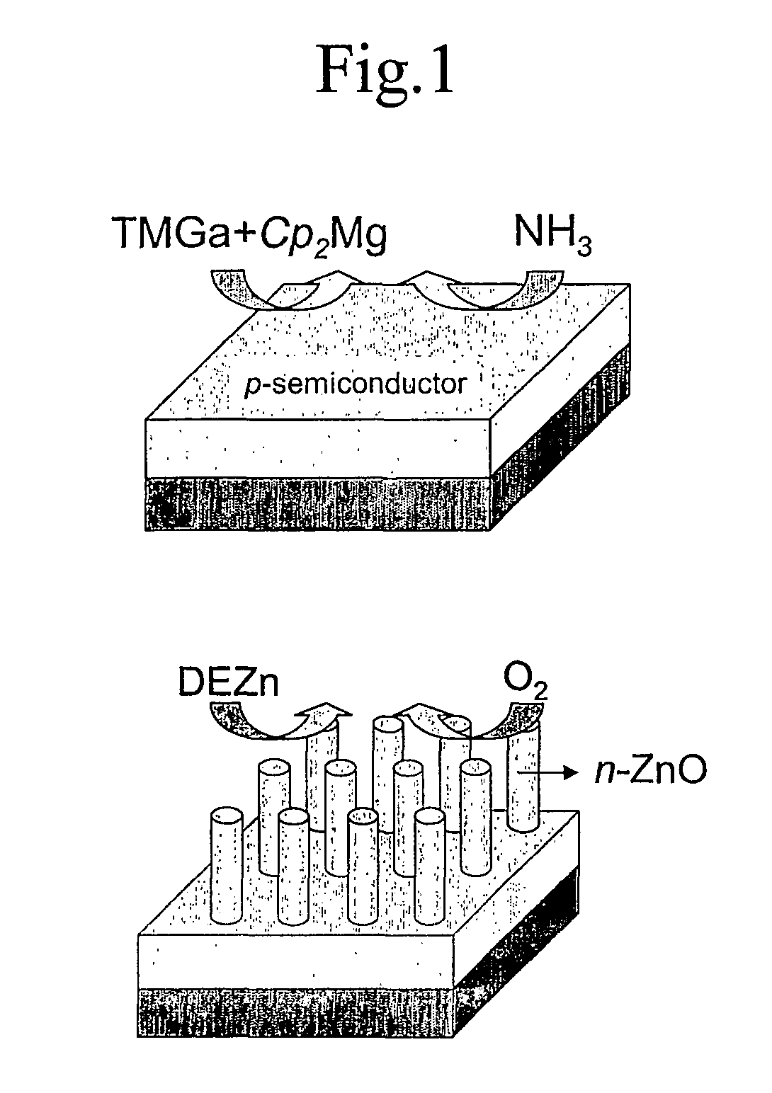
[0033] ZnO-based p-n heterojunction structure was prepared by the process as shown in FIG. 1 as follows.

[0034] An Mg-doped GaN thin film was deposited on an Al2O3 substrate using a conventional MOCVD technique and annealed, to obtain a p-type GaN thin film having a thickness of 2 μm. The metal organic precursors used were trimethylgallium (TMGa) and bis(cyclopentadienyl) magnesium ((C5H5)2Mg); and the nitrogen precursor, NH3.

[0035] Then, n-type ZnO nanorods were vertically grown on the p-type GaN thin film thus obtained, by injecting gaseous Zn(C2H5)2 and O2 at flow rates in the ranges of 1 to 10 sccm and 20 to 100 sccm, respectively, with an argon (Ar) carrier gas and reacting the vapors for about 1 hour, to obtain a p-n heterojunction structure comprising n-ZnO nanorods grown on the p-GaN thin film. The reactor pressure and temperature were maintained in the ranges of 0.1 to 10 torr and 400 to 700° C., respectively, during the...

example 2

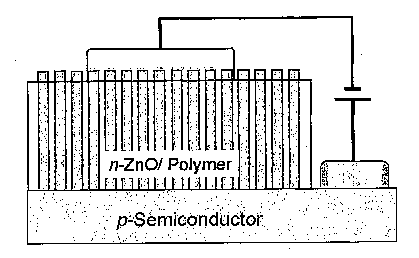
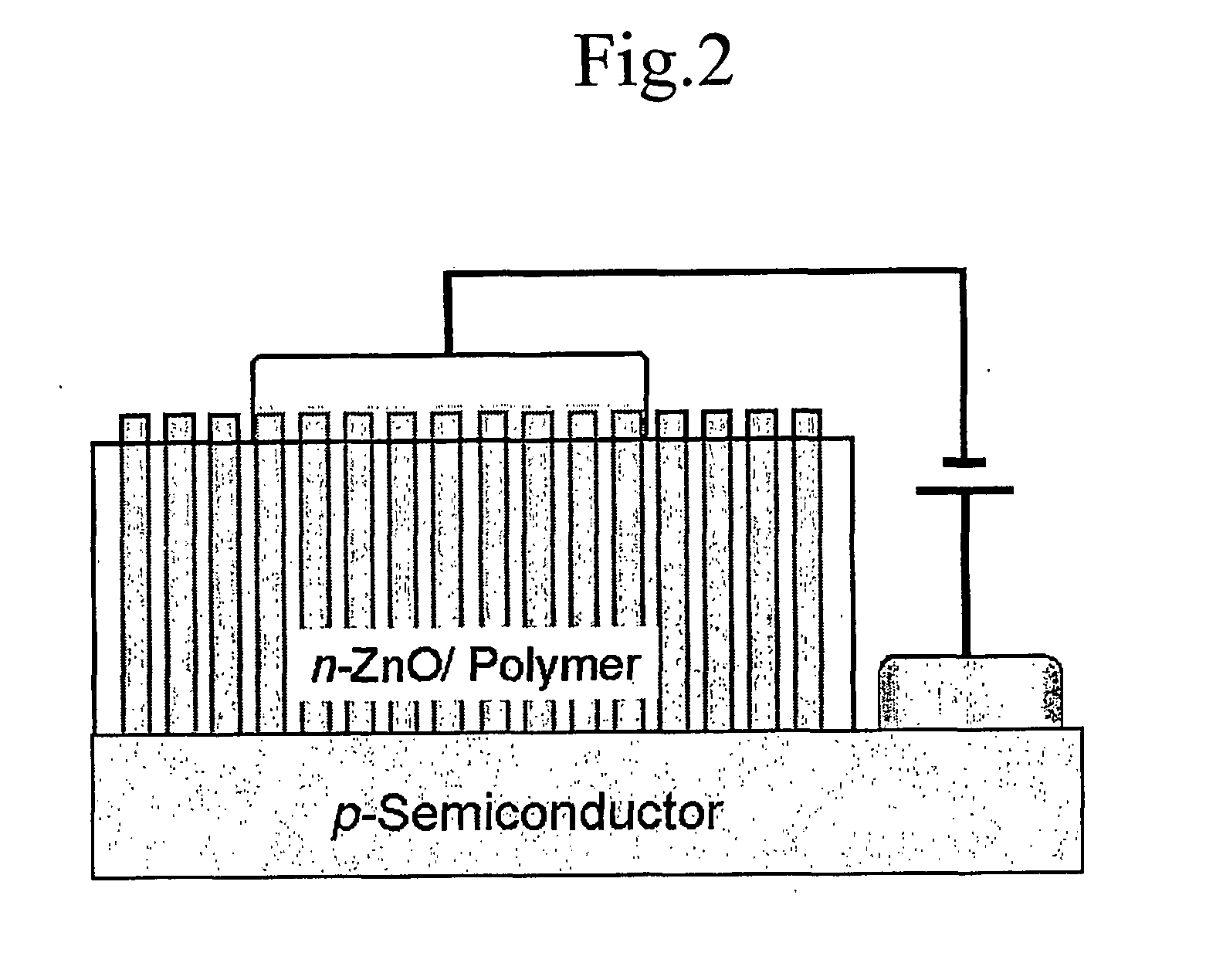
Fabrication of a Light Emitting Diode

[0037] A light emitting diode was fabricated using the heterojunction structure prepared in Example 1 as follows.

[0038] First, the free space around the ZnO nanorods grown on a GaN thin film was filled up by depositing an insulating material (e.g., photoresist, polyimide, etc.) thereon, and then, the tip portion of the nanorods was exposed by etching using a plasma. Subsequently, a Ti (10 nm) / Au (50 nm) top ohimic electrode was formed at the tip portion of the etched n-type nanorods; and a Pt (10 nm) / Au (50 nm) bottom electrode, on the p-type GaN thin film, by a thermal or electron beam evaporation technique. The applied accelerating voltage and emission current were in the ranges of 4 to 20 kV and 40 to 400 mA, respectively, during the electrodes deposition, which was conducted under a reactor pressure of around 10−5 mmHg, while keeping the substrate temperature at room temperature.

[0039] The cross-sectional morphology of the top electrode-fo...


PUM


Abstract

A heterojunction structure composed of a p-type semiconductor thin film and n-type ZnO-based nanorods epitaxially grown thereon exhibits high luminescence efficiency property due to facilitated tunneling of electrons through the nano-sized junction and the use of ZnO having high exciton energy as a light emitting material, and thus it can be advantageously used in nano-devices such as LED, field effect transistor, photodetector, sensor, etc.

Description

FIELD OF THE INVENTION [0001] The present invention relates to a novel heterojunction structure comprising a p-type semiconductor thin film and an n-type ZnO-based nanorod epitaxially grown thereon, which provides a light emitting device having improved luminescence properties. BACKGROUND OF THE INVENTION [0002] The Gallium nitride (GaN)-based blue light emitting diode (LED) developed by Nichia Chemical Co., Ltd. in 1993 uses a GaN p-n thin film junction to provide blue and green LED devices, and in 1997, a short wavelength (404 nm) blue LED having a life span of about 10,000 hours at room temperature has been developed using a nitride semiconductor. [0003] Recently, an n-type oxide semiconductor, zinc oxide (ZnO), has attracted attention as an another efficient light emitting (λ=380 nm) material at room temperature due to its interesting features: (1) a direct transition band structure, (2) a low power threshold for optical pumping at room temperature and (3) a large exciton bindin...

Claims


Application Information

Patent Timeline
IPC IPC(8): H01L21/00H01L33/00C30B29/16C30B29/60H01L21/365H01L29/06H01L29/20H01L29/267H01L33/08H01L33/26H01L33/28
CPCB82Y10/00B82Y30/00C30B29/16C30B29/605H01L21/0237H01L21/02389H01L21/02554H01L21/0256H01L21/02565H01L21/02568H01L21/02576H01L21/02603H01L21/0262H01L21/02639H01L21/02647H01L21/02664H01L29/0665H01L29/0673H01L29/0676H01L29/2003H01L29/267H01L33/08H01L33/26H01L33/28
Inventor YI, GYU-CHULPARK, WON-II
Owner LG DISPLAY CO LTD
Why Eureka
Try Eureka