Etchant and method of etching

a multi-layer film and etching technology, applied in the field ofetc, can solve the problems of increasing the area of the exposed part of the lower metal layer, exceedingly low production efficiency, and failure of insulation resistance, and achieves satisfactory precision, less adhesion, and improved etching function.

Inactive Publication Date: 2006-08-24
MITSUBISHI ELECTRIC CORP +1
View PDF16 Cites 33 Cited by
  • Summary
  • Abstract
  • Description
  • Claims
  • Application Information

AI Technical Summary

Benefits of technology

[0014] The investigations made by the inventors have revealed that the nitric acid in the etchant of the invention probably functions to lessen adhesion between the upper layer comprising a molybdenum-niobium alloy and the edges of the photoresist resin layer overlying the upper layer and thereby accelerate etchant penetration into the interface between these. Namely, the side etching rate of the molybdenum-niobium alloy layer in contact with the photoresist resin layer is heightened in a suitable degree, whereby the etching rate of the molybdenum-niobium alloy layer increases and the etchin...

Problems solved by technology

In the wet etching of multilayer films comprising an aluminum alloy layer and a molybdenum alloy layer superposed thereon as described above, some combinations of metals have resulted in exceedingly low production efficiency, for example, because of the necessity of successively etching the individual layers constituting the multilayer film with two different etchants.
There have been a problem in the parts which suffered ...

Method used


Image

  • Etchant and method of etching
  • Etchant and method of etching

Examples


examples

[0072] The invention will be explained below in more detail by reference to Examples and Reference Examples, but the invention should not be construed as being limited to the following Examples unless the invention departs from the spirit thereof.

examples 1 to 7 and reference examples 1 to 6

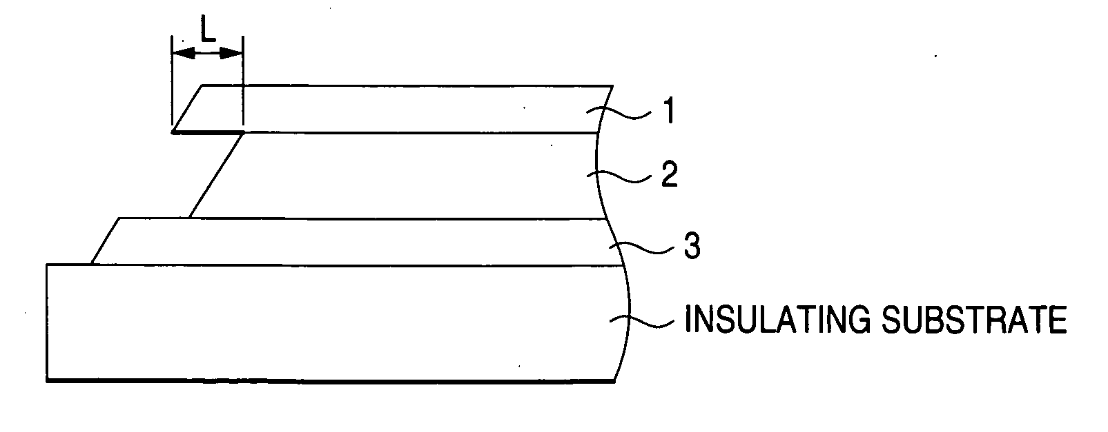
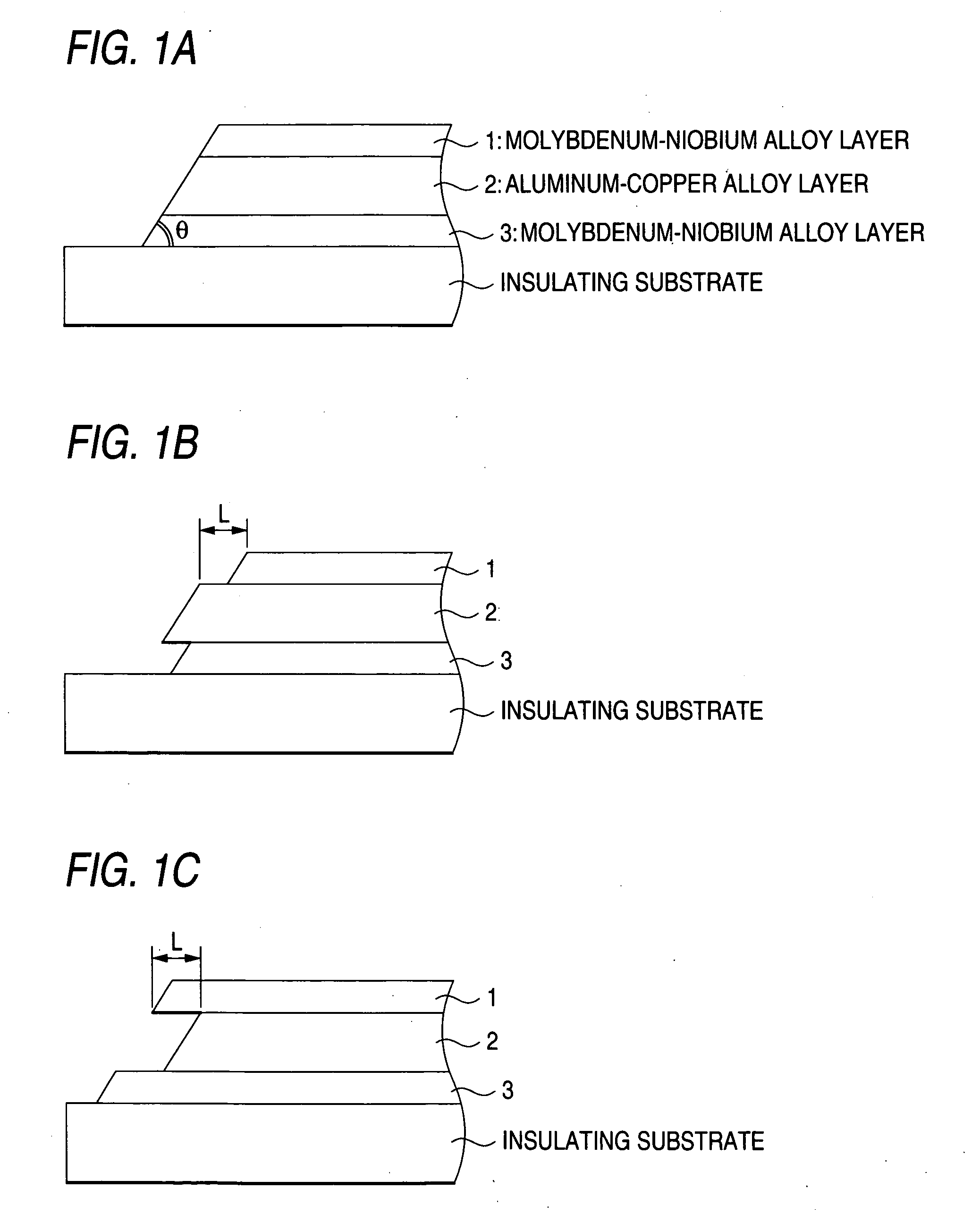
[0073] A molybdenum-niobium alloy layer (niobium content, 5% by weight) 3 having a thickness of 50 nm was deposited on a glass substrate by sputtering. On this layer was deposited AlCu (aluminum-copper alloy; copper content, 5% by weight) in a thickness of 300 nm as an aluminum alloy layer 2 by sputtering using argon gas. Thereafter, a molybdenum-niobium alloy layer 1 having the same composition as shown above and having a thickness of 50 nm was continuously deposited. Thus, an MoNb / AlCu / MoNb multilayer film was formed as shown in FIG. 1A, FIG. 1B, and FIG. 1C.

[0074] A positive photoresist resin layer (thickness, about 1.5 μm) was further formed thereon by spin coating, and this layer was treated by photolithography to form a fine wiring pattern. The line width of this resist pattern was about 5 μm.

[0075] This substrate was cut into pieces having a width of about 10 mm and a length of 50 mm, and these pieces were used as etching test samples.

[0076] On the other hand, a molybdenum...


PUM

PropertyMeasurementUnit
Percent by massaaaaaaaaaa

Abstract

A fine wiring line profile with satisfactory precision is formed from a multilayer film containing a first layer made of an aluminum alloy and a second layer formed thereon made of a molybdenum-niobium alloy, by simultaneously etching the two layers constituting the multilayer film through only one etching operation while preventing the upper layer from forming overhangs. An etchant for etching a multilayer film containing an aluminum alloy layer formed over a substrate and a molybdenum-niobium alloy layer formed thereon having a niobium content of 2-19% by weight contains an aqueous solution of an acid mixture containing phosphoric acid, nitric acid, and an organic acid; and a method of etching is carried out with this etchant. The etchant preferably has a phosphoric acid concentration Np of 50-75% by weight, a nitric acid concentration Nn of 2-15% by weight, and an acid ingredient concentration defined by Np+(98/63)Nn of 55-85% by weight.

Description

TECHNICAL FIELD [0001] The present invention relates to an etchant for use in patterning thin metal films by wet etching and to a method of etching with the same. More particularly, the invention relates to an etchant and an etching method for etching a multilayer film comprising an aluminum alloy layer and a molybdenum-niobium alloy layer. BACKGROUND ART [0002] Recently, electrodes and gate wiring materials for use in semiconductor devices such as semiconductor elements and liquid-crystal display elements are increasingly required to have a higher degree of precision in microfabrication. In addition, it has been proposed to use metallic materials having a lower resistance. Examples of metallic materials having a low resistance include aluminum and aluminum alloys, and these materials are coming to be used increasingly. [0003] Examples of techniques for processing a thin film of such a metal to form a pattern of a microstructure such as a wiring include wet etching techniques in whi...

Claims


Application Information

Patent Timeline
IPC IPC(8): H01L21/4763H01L21/302C23F1/20C23F1/26C23F1/44H01L21/28H01L21/306H01L21/3205H01L21/3213H01L21/768H01L23/52
CPCC23F1/20C23F1/26C23F1/44H01L21/32134
Inventor SAITOU, NORIYUKIYOSHIDA, TAKUJIINOUE, KAZUNORIISHIKAWA, MAKOTOKAMIHARAGUCHI, YOSHIO
Owner MITSUBISHI ELECTRIC CORP
Why Eureka
Try Eureka