

Method for applying metal features onto barrier layers using ion permeable barriers
a technology of ion permeable barriers and metal features, which is applied in the direction of electrolytic processes, semiconductor devices, electrolysis components, etc., can solve the problems of difficult effective and economical depositing of copper metallization, high cost of cvd, and high equipment costs, so as to avoid time-consuming pvd or cvd, avoid the cost of metallization, and increase the effect of throughpu
- Summary
- Abstract
- Description
- Claims
- Application Information
AI Technical Summary
Benefits of technology
Problems solved by technology
Method used
Image

Examples
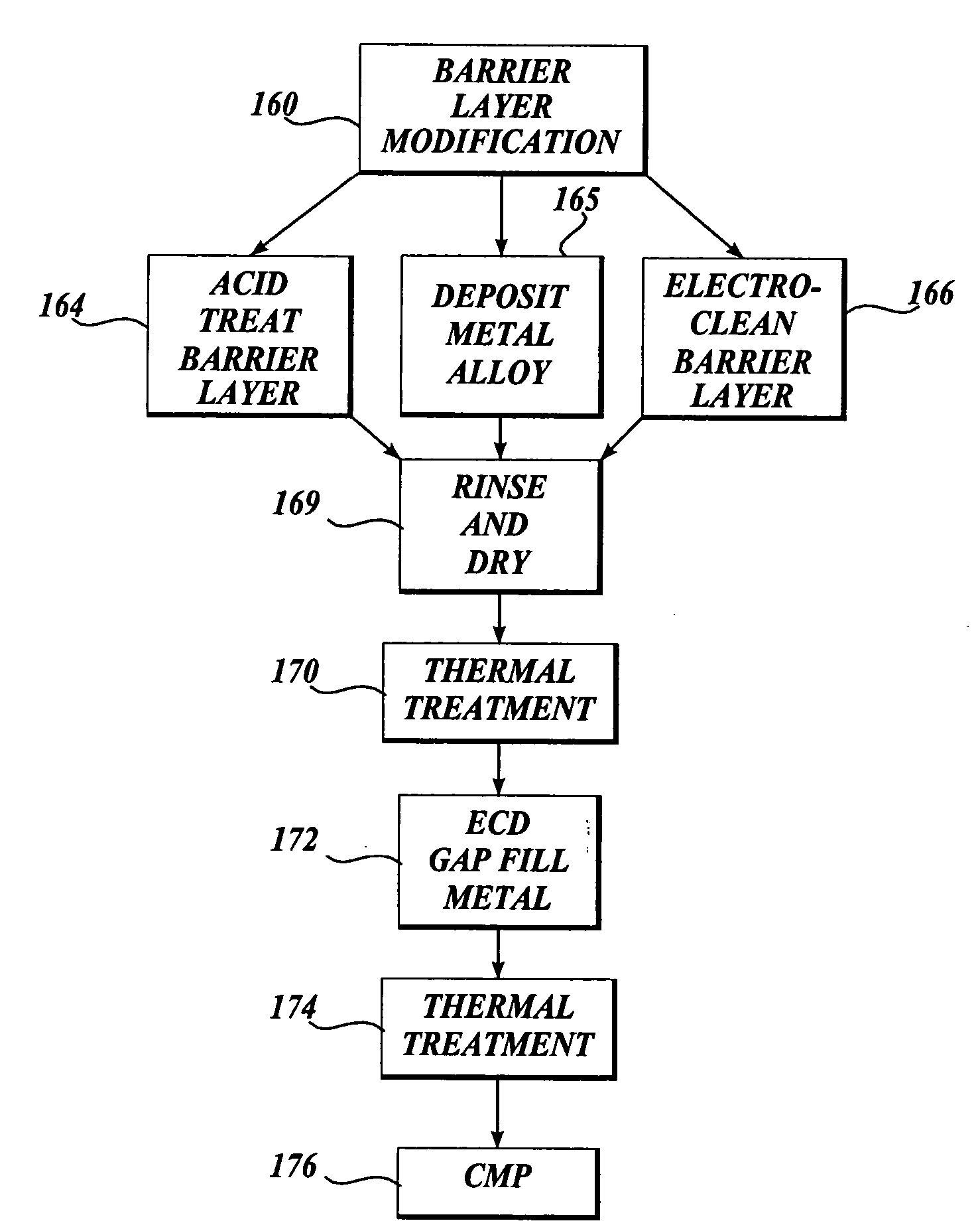
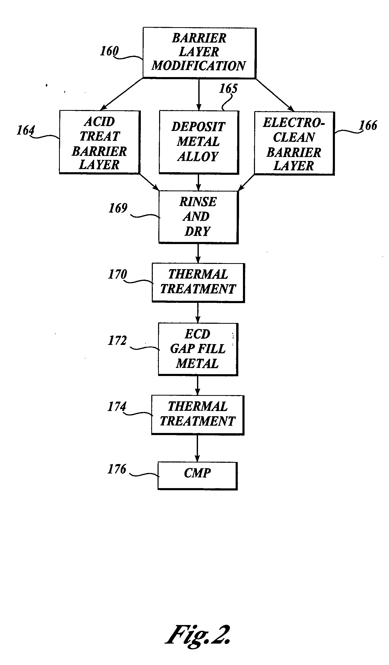
example 1
[0167] Acid Treatment of Barrier Layer
[0168] Acid treatment of a tantalum barrier was performed using 2% by weight aqueous solution of hydrofluoric acid. A 200 mm blanket wafer deposited with 25 nanometers of PVD tantalum barrier was used. This rotating wafer was subjected to a water spray treatment for 15 seconds followed by an acid spray treatment for 15 seconds. Then the rotating wafer was cleaned by spraying de-ionized water for another 15 seconds to remove the excess acid from its surface. For an additional 5 seconds, the wafer was rotated to sling off large water droplets. The wafer was then wet-transferred to a plating chamber. In the plating chamber, the wafer was plated with copper up to a thickness of ˜80 nanometers. After plating, the wafer was cleaned in situ with de-ionized water and the wafer was transferred to a SRD (Spin, Rinse, and Dry) chamber. In this SRD chamber, the spinning wafer was once again cleaned with de-ionized water thoroughly to remove any plating che...
example 2
[0169] Electrolytic Treatment of Barrier Layer
[0170] Electrolytic treatment of a tantalum barrier was performed using 2% by weight of potassium hydroxide aqueous solution. A 200 mm blanket wafer with 25 nanometers of PVD tantalum barrier was treated. This rotating wafer was used as a cathode and subjected to a current of 1 A (˜3 mA / cm2) for one minute while an inert platinum electrode was the anode. The wafer was then wet-transferred to a SRD chamber where the spinning wafer was rinsed with de-ionized water and then once again wet transferred to a plating chamber. In the plating chamber, the wafer was plated with copper up to a thickness of about 80 nanometers. After plating, the wafer was cleaned in situ with de-ionized water and the wafer was transferred to a SRD chamber. In this SRD chamber, the spinning wafer was once again cleaned with de-ionized water thoroughly to remove any plating chemistry left on its surface. After rinsing, the wafer was dried by spinning it in the chamb...
PUM
| Property | Measurement | Unit |
|---|---|---|
| Fraction | aaaaa | aaaaa |
| Percent by mass | aaaaa | aaaaa |
| Percent by mass | aaaaa | aaaaa |
Abstract
Description
Claims
Application Information