Electrode step difference offsetting print paste and production method for electronic components

a production method and electronic component technology, applied in the direction of electrical equipment, domestic applications, inks, etc., can solve the problems of deformation of stacked bodies, delamination between sheets, etc., and extremely low viscosity of dielectric paste, so as to achieve excellent mechanical strength, effective delamination prevention, and excellent adhesiveness

Inactive Publication Date: 2006-08-31
TDK CORPARATION
View PDF3 Cites 31 Cited by
  • Summary
  • Abstract
  • Description
  • Claims
  • Application Information

AI Technical Summary

Benefits of technology

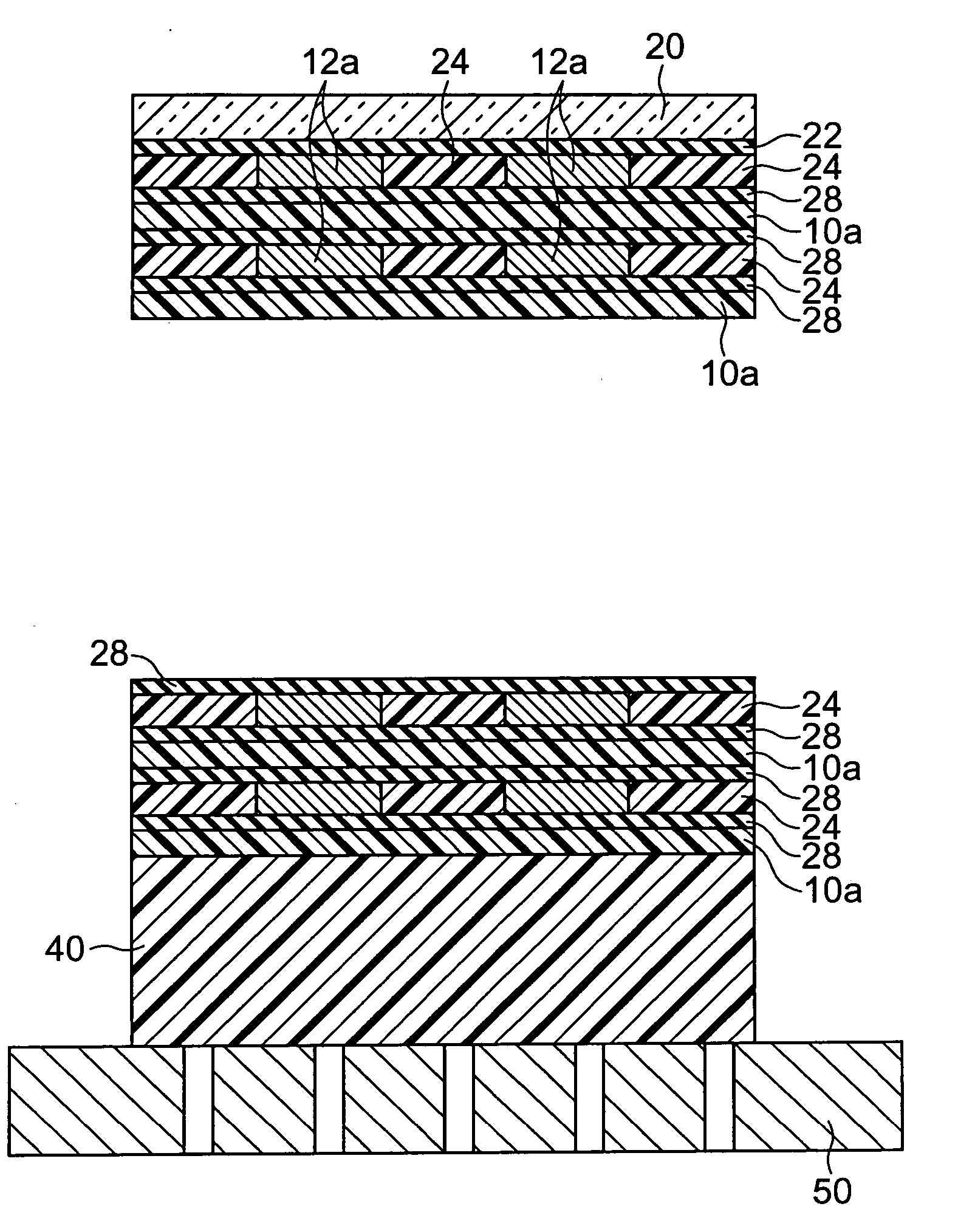
[0011] An object of the present invention is to provide an electrode level difference absorbing print paste (a paste for forming a blank pattern) for printing a thin film, capable of forming a print material having excellent mechanical strength and adhesiveness. Specifically, an object of the present invention is to provide an electrode level difference absorbing print paste capable of preferably eliminate a level difference of an electrode layer between green sheets and effectively preventing delamination between sheets and deformation of a stacked body even when a thickness of the green sheet and / or electrode layer is extremely thin, and a method of producing an electronic device. Furthermore, an object of the present invention is to provide an electrode level difference absorbing print paste for forming a blank pattern having excellent adhesiveness particularly when forming a stacked body of green sheets and electrode layers by a transfer method.
[0012] The present inventors have been committed themselves to study to attain the above objects, found that it was possible to preferably eliminate a level difference of an electrode layer between green sheets and prevent delamination between sheets and deformation of a stacked body, etc. even when a thickness of the green sheet and / or electrode layer is extremely thin by making a polyvinyl butyral resin having a certain polymerization degree contained in a paste used for forming a blank pattern layer of an internal electrode layer as a binder resin, and completed the present invention.
[0016] According to the electrode level difference absorbing print paste according to the present invention, it becomes possible to preferably print even an extremely thin blank pattern layer without extremely declining viscosity of the electrode level difference absorbing print paste. Also, it is not necessary to increase an amount of a binder resin included in the electrode level difference absorbing print paste, so that there is a low possibility of causing delamination between sheets, etc. at the time of binder removal of the stacked body.
[0017] Preferably, a polymerization degree of a binder resin included in the electrode level difference absorbing-print paste is 1400 or more, more preferably 1700 or more, and particularly preferably 2000 or more. By using a binder resin having a polymerization degree as such, strength of a blank pattern layer is improved, strength of an electrode added sheet as a whole is improved, and handlability can be widely improved. Note that the upper limit of the polymerization degree of the binder resin is not particularly limited but is, for example, 3300 or so.
[0047] Preferably, the binder resin included in the electrode level difference absorbing print paste and the binder resin included in slurry for forming the green sheets are the same kind. Due to this, an improvement of adhesiveness between the green sheets and setting of a condition of binder removal processing become easy.

Problems solved by technology

Due to the blank pattern, there arises a level difference from portions where the internal electrode layer exists, consequently, delamination between sheets and deformation of a stacked body, etc. become problems.
However, in this case, viscosity of the dielectric paste extremely declines, so that there arises a problem that the paste flows out from a mesh of a print plate making and printing in a predetermined pattern becomes impossible.
However, in this case, there is a problem that delamination, etc. arises between sheets when performing binder removal on the stacked body.
Furthermore, in the case of forming an extremely thin blank pattern, when a conventionally general ethyl cellulose based resin is used as the binder resin of the paste, there are also problems that the strength declines and adhesive force declines as the layer becomes thinner as the layer becomes thinner.

Method used


Image

  • Electrode step difference offsetting print paste and production method for electronic components
  • Electrode step difference offsetting print paste and production method for electronic components
  • Electrode step difference offsetting print paste and production method for electronic components

Examples


example 1

[0153] Production of Green Sheet Paste

[0154] As a starting material of ceramic powder, BaTiO3 powder (BT-02 made by Sakai Chemical Industry Co., Ltd.) was used. A ceramic powder subcomponent additives were prepared to satisfy (Ba0.6Ca0.4)SiO3: 1.48 parts by weight, Y2O3: 1.01 parts by weight, MgCO3: 0.72 wt %, Cr2O3: 0.13 wt % and V2O5: 0.045 wt % with respect to 100 parts by weight of the BaTiO3 powder.

[0155] First, only the subcomponents were mixed by a ball-mill to obtain slurry. Namely, the subcomponent additives (total amount 8.8 g) and a solvent (16 g), wherein ethanol / n-propanol is 1:1, were preliminary ground by a ball-mill for 20 hours. Next, the preliminary ground slurry of the subcomponent additives, ethanol: 38 g, n-propanol: 38 g, xylene: 28 g, mineral spirit: 14 g, DOP (dioctyl phthalate) as a plasticizer component: 6 g and a polyethylene glycol based nonionic dispersant (HLB=5 to 6) as a dispersant: 1.4 g were added to BaTiO3: 191.2 g and mixed by a ball-mill for 4 ...

reference example 1

[0190] Other than changing the weight percentage of the ceramic powder in the paste to less than 30 wt %, which is lower than the lower limit of the preferable range of the present invention, an electrode level difference absorbing print paste was produced in the same as in the example 1. As a result, due to a decline of the paste viscosity, a disadvantage that the paste flows out from a mesh of a print plate making was observed.

example 2

[0191] As shown in Table 2 below, other than using a polyvinyl butyral resin having a polymerization degree of 1700 as a binder resin, electrode level difference absorbing print pastes of sample numbers 10 to 17 were produced, and viscosity of the paste and the minimum possible print thickness by the printing method were examined.

[0192] The results are shown in Table 2. As shown in Table 2, pigment concentration of 38 to 50 wt % was preferable when the polymerization degree was 1700.

TABLE 2Polymer-ResinPigmentButyralationAcetalizationPlasticizerAntistaticViscosityPrintizationAmountConcentrationDegreeDegreeAmountAgent[Pa · s]ThicknessDegree[php][wt. %][mol. %][mol. %][phr]Kind(at 8[1 / s])[μm]Sample1017006306950Imidazoline Base10.7Sample111700↓34↓↓↓30.8Sample121700↓38↓↓↓51Sample131700↓42↓↓↓91.2Sample141700↓46↓↓↓171.6Sample151700↓50↓↓↓292.1Sample161700↓54↓↓↓45Sample171700↓58↓↓↓70


PUM

PropertyMeasurementUnit
viscosityaaaaaaaaaa
thicknessaaaaaaaaaa
thicknessaaaaaaaaaa

Abstract

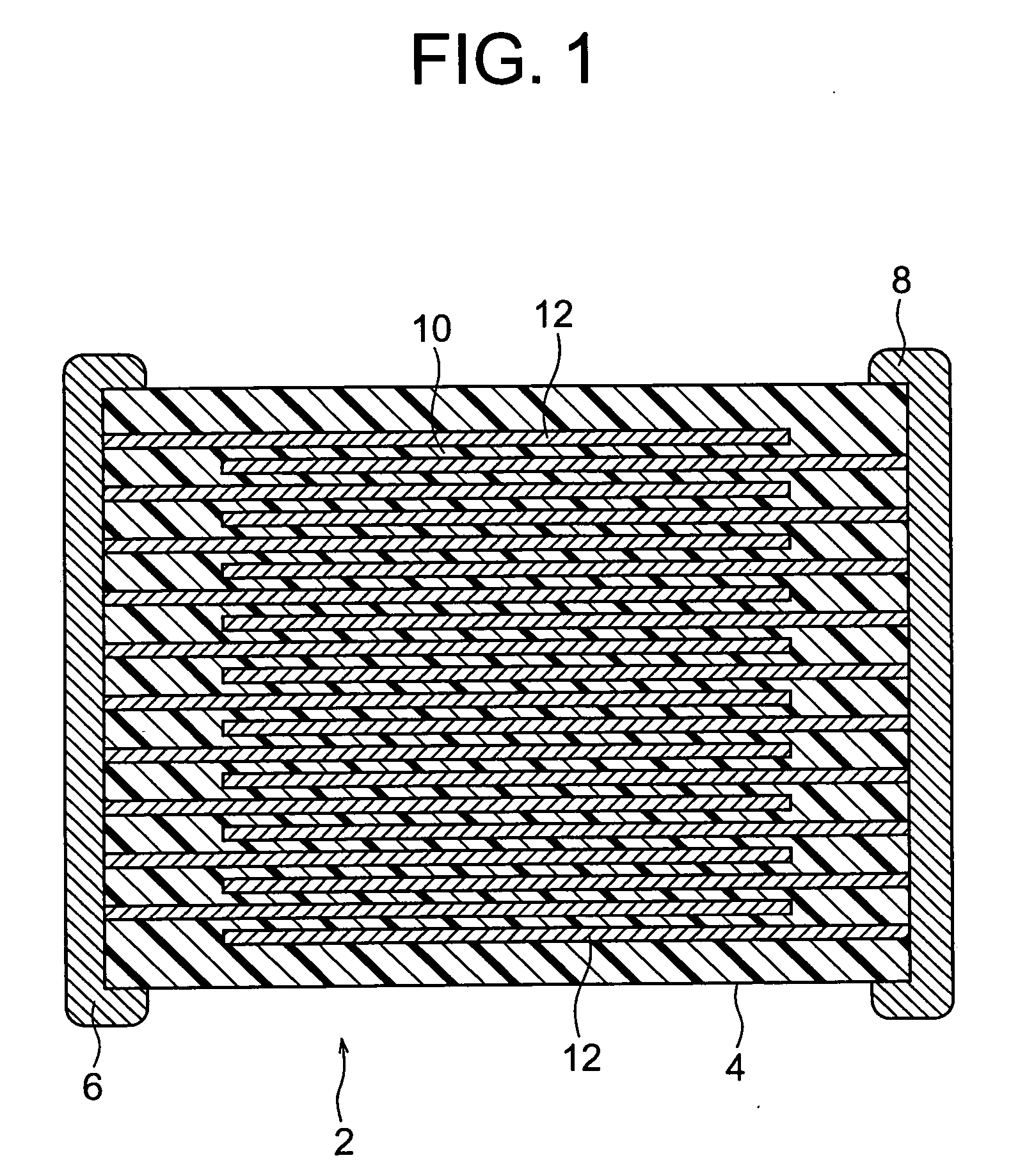
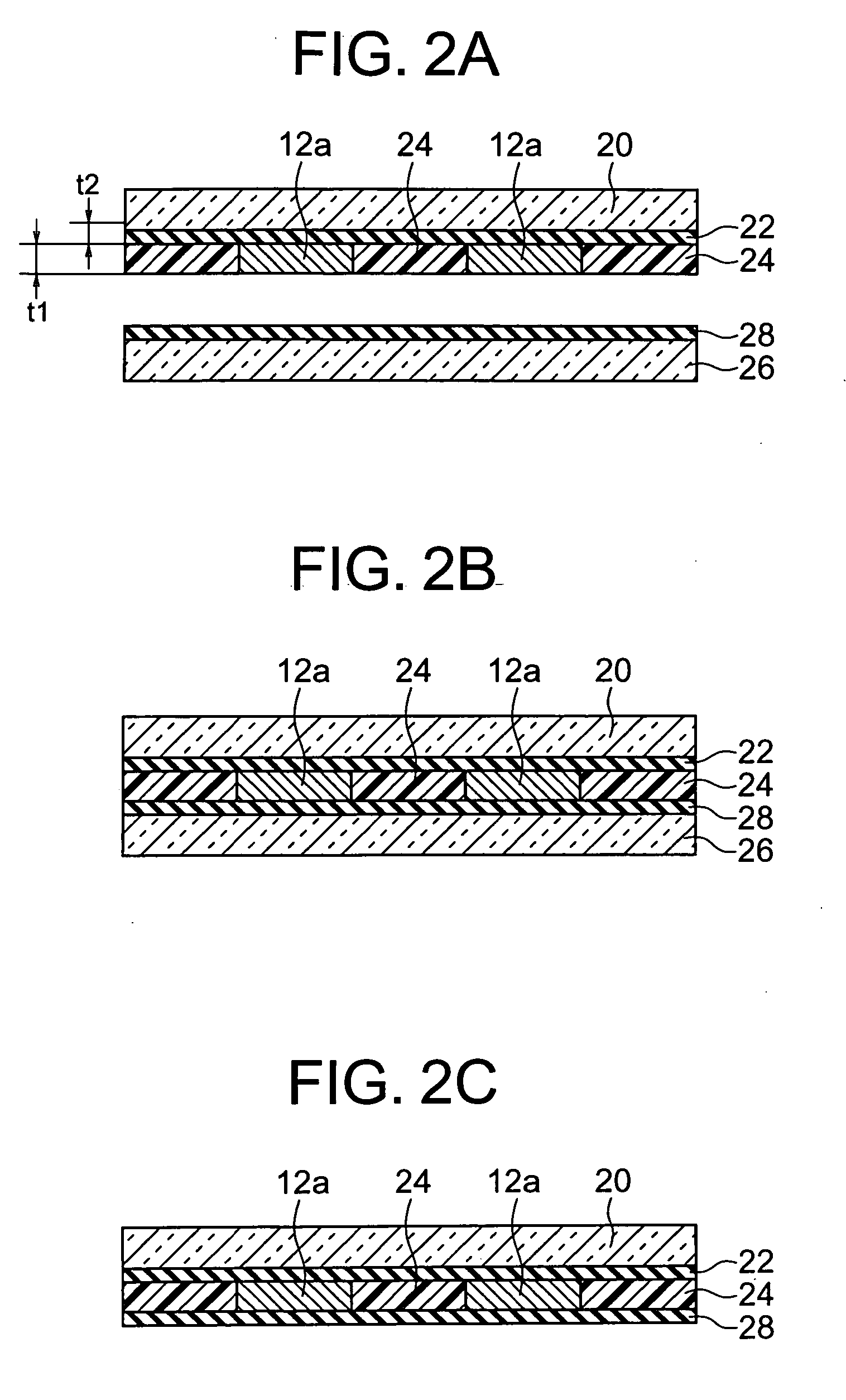
A production method of an electronic device comprising the steps of forming a stacked body by stacking green sheets 10a and electrode layers 12a having a predetermined pattern and firing the stacked body. Before forming the stacked body, a blank pattern layer 24 having substantially the same thickness as that of the electrode layer is formed on a space portion of the electrode layer having a predetermined pattern. The electrode level difference absorbing print paste for forming the blank pattern layer 24 includes at least ceramic powder and a binder resin, and a polymerization degree of the binder resin included in the electrode level difference absorbing print paste is made equal to or more than that of a binder resin included in slurry for forming the green sheet. The binder resin of the electrode level difference absorbing print paste includes a polyvinyl butyral resin, a polymerization degree of the polyvinyl butyral resin is 1400 or more, a butyralation degree is 64 to 74 mol %, and an acetalization degree is 66 to 74 mol %.

Description

TECHNICAL FIELD [0001] The present invention relates to a production method of an electronic device, such as a multilayer ceramic capacitor. BACKGROUND ART [0002] In recent years, as a variety of electronic equipments become compact, electronic devices to be installed inside the electronic equipments have become more compact and higher in performance. As one of the electronic devices, there is a ceramic electronic device, such as a CR built-in substrate and a multilayer ceramic capacitor, and the ceramic electronic devices have been required to be more compact and higher in performance. [0003] To pursue a more compact ceramic electronic device having a higher capacity, there is a strong demand for making a dielectric layer thinner. Recently, a thickness of a dielectric green sheet composing a dielectric layer has become a several μm or less. [0004] To produce a multilayer ceramic capacitor, an interlayer thickness of a sheet formed with an internal electrode is in a range of about 3...

Claims


Application Information

Patent Timeline
Patent Type & Authority Applications(United States)
IPC IPC(8): C04B14/48B29C69/00C04B35/468C04B35/634H01G4/12H01G4/30
CPCC04B35/4682H01G4/30C04B35/63C04B35/632C04B35/6342C04B35/63488C04B2235/3206C04B2235/3215C04B2235/3225C04B2235/3236C04B2235/3239C04B2235/3241C04B2235/3436H01G4/12C04B35/6264H01G5/011C08G2/24
Inventor YAMAGUCHI, AKIRASATOU, SHIGEKITOKUOKA, YASUMICHI
Owner TDK CORPARATION
Why Eureka
Try Eureka