Method of forming electronic devices

a technology of electronic devices and masks, applied in the direction of printed circuit aspects, sustainable manufacturing/processing, final product manufacturing, etc., can solve the problems of solder joint fatigue, solder joint almost always fails at the interface between the solder joint and the solder mask, and the stress on the solder joint that connects the device and the printed circuit board,

Inactive Publication Date: 2006-08-31
GENERAL ELECTRIC CO
View PDF8 Cites 18 Cited by
  • Summary
  • Abstract
  • Description
  • Claims
  • Application Information

AI Technical Summary

Problems solved by technology

The solder joints that connect the device and the printed circuit board are subject to thermomechanical stresses during device operation, due to differences in coefficients of thermal expansion (CTE) between the device and the printed circuit board.
Thus, the primary mode of failure is solder joint fatigue.
The solder joints almost always fail at the solder joint-solder mask interface towards the device side, due to stress concentrations arising from a solder mask defined (SMD) attachment pad on the device side.
These processes add cost to the final product.

Method used


Image

  • Method of forming electronic devices
  • Method of forming electronic devices
  • Method of forming electronic devices

Examples


example 1

Preparation of functionalized colloidal silica (FCS) predispersion.

[0067] A functionalized colloidal silica predispersion was prepared by combining the following: 935 grams of isopropanol (Aldrich) was slowly added by stirring to 675 grams of aqueous colloidal silica (Nalco 1034A, Nalco Chemical Company or Snowtex OL, Nissan Chemical Co.,) containing 34 weight % of 20 nanometer particles of SiO2 (Nalco 1034A) or 21 weight % of 50 nanometer SiO2 particles (Snowtex OL). Subsequently, phenyl trimethoxysilane (PTS, 58.5 grams for Nalco 1034A, 22.0 grams for Snowtex OL ), (Aldrich), which was dissolved in 100 grams isopropanol, was added to the stirred mixture. The mixture was then heated to 80° C. for 1-2 hours to afford a clear suspension. The resulting suspension of functionalized colloidal silica was stored at room temperature. Multiple dispersions based on Nalco 1034 (see Table 1), having various levels of SiO2 (from 10% to 30% by weight) were prepared for use in Example 2.

example 2

Preparation of a concentrated dispersion of functionalized colloidal silica in methoxypropanol.

[0068] A 2000 milliliter flask round bottom was charged with 540 grams of each of the pre-dispersions, prepared in Example 1. Additional pre-dispersion compositions are shown in Table 1, below. 1-methoxy-2-propanol (750 grams) was then added to each flask. The resulting dispersion of functionalized colloidal silica was vacuum stripped at 60° C. and 60 millimeter Hg to remove about 1 liter of solvents. The vacuum was slowly decreased and solvent removal continued with good agitation until the dispersion weight had reached 140 grams in the case of materials based on Nalco 1034A or 80 grams for Snowtex OL cases. The clear dispersions of phenyl-functionalized colloidal silica contained 50% by weight SiO2 and no precipitated silica. These dispersions were stable at room temperature for more than three months. The results in Table 1 show that a certain level of phenyl functionality is required...

example 3

Preparation of a dispersion of capped functionalized colloidal silica in epoxy resin.

[0069] A solution of 3.2 grams of epoxy cresol novolac (ECN 195XL-25 available from Sumitomo Chemical Co.), 1.84 grams of Epon 826 (available from Resolution Performance Products), 2.6 grams of novolac hardener (Tamanol 758 available from Arakawa Chemical Industries) in 3.0 grams of 1-methoxy-2-propanol was heated to about 50° C. A 7.12 grams portion of the solution was added, dropwise, to 10.0 grams of the FCS dispersion (see Table 1, entry #3, 50% SiO2 in methoxypropanol), by stirring at 50° C. followed by additional methoxypropanol (3.6 grams). The clear suspension was cooled and a catalyst solution of N-methylimidazole, 60 microliters of a 25% w / w solution in methoxypropanol was added by stirring.

Test procedure:

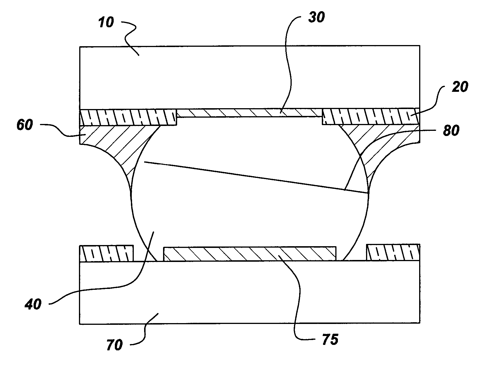
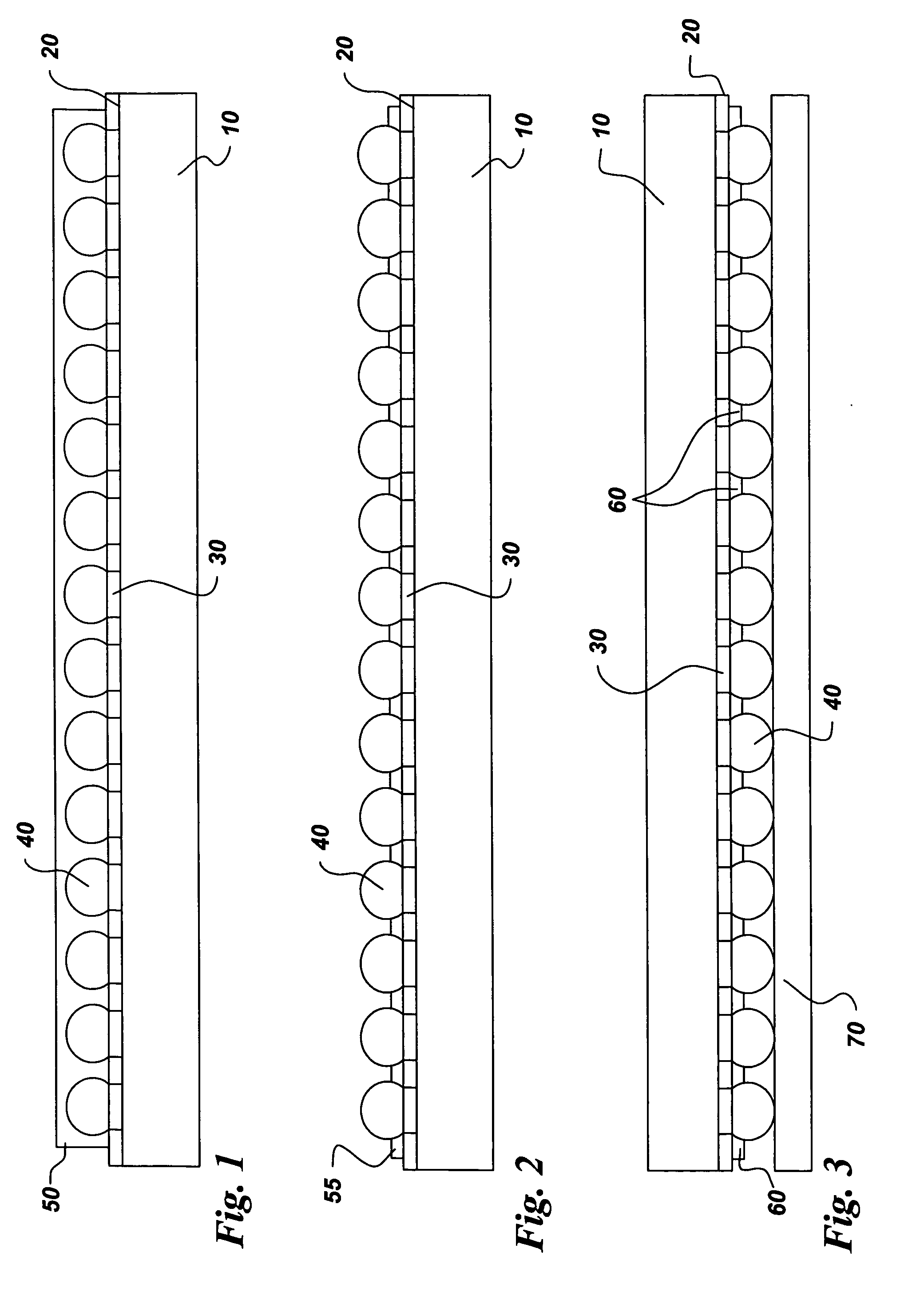
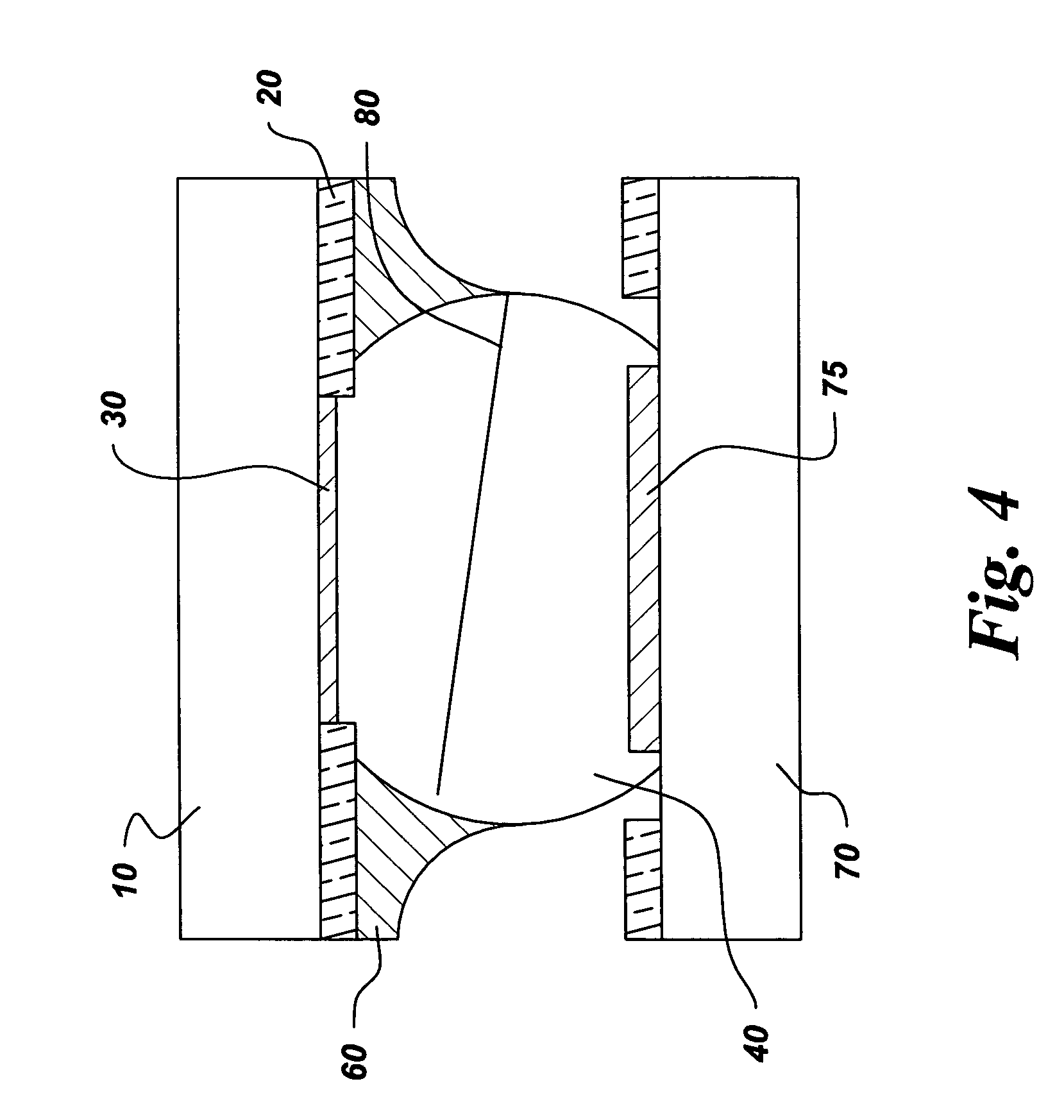
[0070] The test part used to demonstrate the reliability improvement from the polymer reinforcement system was an electronic device classified as a Wafer Level Chip Scale Package (WL...


PUM

PropertyMeasurementUnit
particle sizeaaaaaaaaaa
viscosityaaaaaaaaaa
particle sizeaaaaaaaaaa

Abstract

A method of forming polymer reinforced solder-bumped containing device or substrate is described. The method comprises the following steps: providing a device or substrate having at least one solder bump formed thereon; coating a predetermined portion of the device or substrate with a curable polymer reinforcement material forming a layer on the device or substrate, partially curing the curable polymer reinforcement material to provide a solder-bumped structure comprising a partially cured polymer reinforcement material, and, making a connection between the solder-bumped structure formed and a printed circuit board or array of attachment pads and fully curing the partially cured polymer reinforcement material to provide a reinforced interconnection. Full curing of the polymer reinforcement material may take place either during the “reflow step” or subsequent to it (post-curing).

Description

BACKGROUND OF THE INVENTION [0001] This invention is related to a method of forming an electronic device comprising a reinforced interconnection. In one aspect, this invention relates to a filled, curable polymer material for solder joint reinforcement in solder-bumped devices. [0002] Demand for smaller and more sophisticated electronic devices continues to drive the electronic industry towards improved integrated circuit packages that are capable of supporting higher input / output density as well as have enhanced performance at smaller device areas. To cope with such a requirement, an arrangement involving a large number of devices joined to the printed circuit board through solder joints disposed in a grid like arrangement on connecting terminals is typically used. The reliability of these solder joints is a function of various design, material, and process factors, including the silicon chip size within the device, printed circuit board thickness, and assembly parameters. The sold...

Claims


Application Information

Patent Timeline
Patent Type & Authority Applications(United States)
IPC IPC(8): H01L23/48H01L21/58
CPCH01L23/49816H05K3/3436H05K2201/0209H05K2201/10977H01L2924/0002H01L2924/00Y02P70/50
Inventor ESLER, DAVID RICHARDBUCKLEY, DONALD JOSEPH JR.TONAPI, SANDEEP SHRIKANTCAMPBELL, JOHN ROBERTMILLS, RYAN CHRISTOPHERPRABHAKUMAR, ANANTHGOWDA, ARUN VIRUPAKSHA
Owner GENERAL ELECTRIC CO
Why Eureka
Try Eureka