Structure and method of fabricating a hybrid substrate for high-performance hybrid-orientation silicon-on-insulator CMOS devices

a technology of hybrid substrates and silicon-on-insulators, applied in the direction of semiconductor devices, basic electric elements, electrical appliances, etc., can solve the problems of significant deformation of electron mobilities on (110) si surfaces, undesirable width of pfets, and completely inappropriate orientation of nfet devices, so as to improve the performance of creating soi-like devices and enhance the performance of each type of devices

Inactive Publication Date: 2006-08-31
GLOBALFOUNDRIES INC
View PDF6 Cites 39 Cited by
  • Summary
  • Abstract
  • Description
  • Claims
  • Application Information

AI Technical Summary

Benefits of technology

[0010] The present invention provides a method of integrating semiconductor devices such that different types of devices are formed upon a specific crystal orientation of a hybrid substrate that enhances the performance of each type of device. Specifically, the present invention provides a method of integrating semiconductor devices (i.e., pFETs and nFETs) such that the pFETs are located on a (110) crystallographic plane, while the nFETs are located on a (

Problems solved by technology

To compensate for this discrepancy, pFETs are typically designed with larger widths in order to balance pull-up currents against the NFET pull-down currents and achieve uniform circuit switching. pFETs having larger widths are undesirable since they take up a significant amount of chip area.
Unfortunately

Method used


Image

  • Structure and method of fabricating a hybrid substrate for high-performance hybrid-orientation silicon-on-insulator CMOS devices
  • Structure and method of fabricating a hybrid substrate for high-performance hybrid-orientation silicon-on-insulator CMOS devices
  • Structure and method of fabricating a hybrid substrate for high-performance hybrid-orientation silicon-on-insulator CMOS devices

Examples


Embodiment Construction

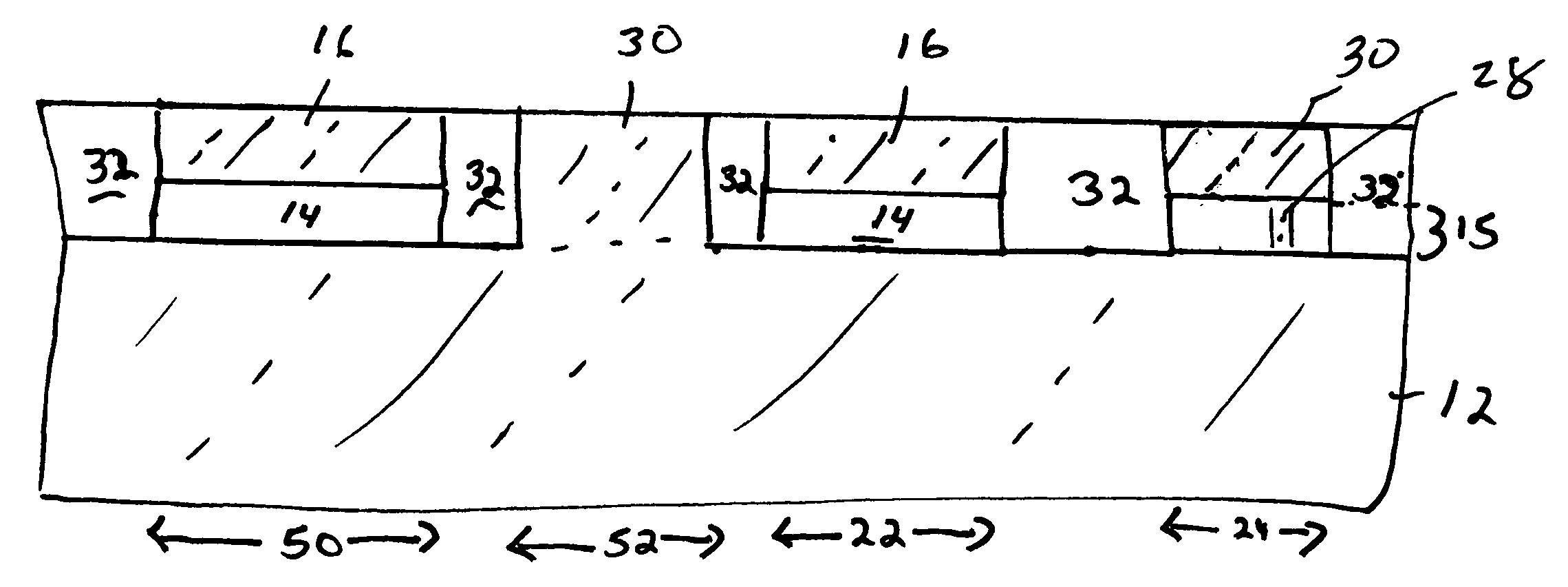
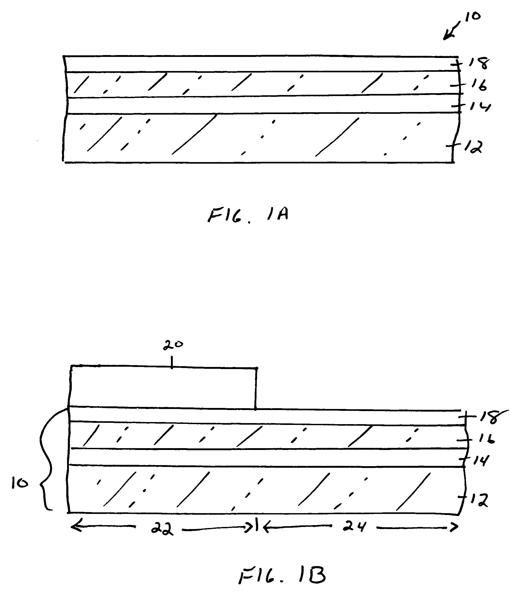
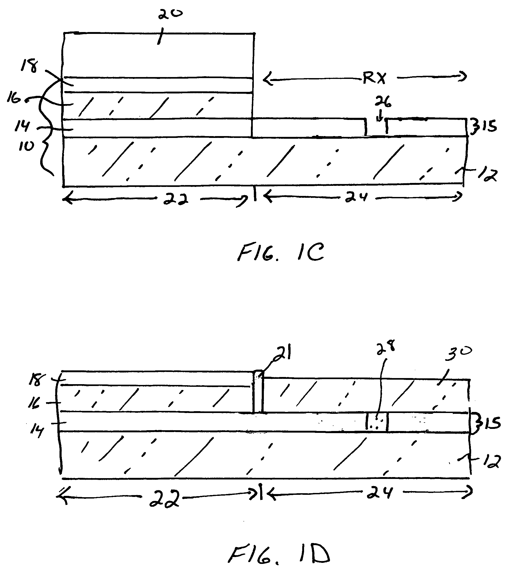
[0032] The present invention will now be described in greater detail by referring to the drawings that accompany the present application. The drawings are provided for illustrative purposes and thus the same are not drawn to scale. It is noted that in the drawings and description provided below, the counter-doped region is formed into the second semiconductor region. Although this embodiment is described and illustrated, the present invention also contemplates forming the counter-doped region into the first semiconductor region rather than the second. Also, although the drawings show the presence of one counter-doped region, the present invention contemplates forming more than one counter-doped region.

[0033] Reference is first made to FIGS. 1A-1G which illustrate the basic processing steps used in the present invention for providing the inventive semiconductor structures, e.g., hybrid substrate and CMOS devices on said hybrid substrate. The inventive process begins by providing sub...


PUM


Abstract

The present invention provides a method of integrating semiconductor devices such that different types of devices are formed upon a specific crystal orientation of a hybrid substrate that enhances the performance of each type of device. Specifically, the present invention provides a method of integrating semiconductor devices such that pFETs are located on a (110) crystallographic plane, while nFETs are located on a (100) crystallographic plane of a planar hybrid substrate. The method of the present invention also improves the performance of creating SOI-like devices with a combination of a buried insulator and counter-doping layers. The present invention also relates to semiconductor structures that are formed utilizing the method of the present invention.

Description

FIELD OF THE INVENTION [0001] The present invention relates to high-performance metal oxide semiconductor field effect transistors (MOSFETs) for digital or analog applications, and more particularly to MOSFETs utilizing carrier mobility enhancement from surface orientation and parasitic and leakage reduction from semiconductor-on-insulator (SOI) structures. BACKGROUND OF THE INVENTION [0002] In present semiconductor technology, complementary metal oxide semiconductor (CMOS) devices, such as nFETs or pFETs, are typically fabricated upon semiconductor wafers, such as Si, that have a single crystal orientation. In particular, most of today's semiconductor devices are built upon Si having a (100) crystal orientation. [0003] On one hand, electrons are known to have a high surface mobility for a (100) Si surface orientation, but holes are known to have high mobility for a (110) surface orientation. That is, hole mobility values on (100) Si are roughly 2×-4× lower than the corresponding el...

Claims


Application Information

Patent Timeline
IPC IPC(8): H01L21/00
CPCH01L21/823807H01L21/823878Y10S438/973H01L27/1203H01L27/1207H01L21/84
Inventor IEONG, MEIKEIYANG, MIN
Owner GLOBALFOUNDRIES INC
Why Eureka
Try Eureka