

Method of forming through hole and method of manufacturing electronic circuit
a technology of electronic circuit and through hole, which is applied in the direction of superimposed coating process, liquid/solution decomposition chemical coating, resistive material coating, etc., can solve the problems of large amount of expensive resist to be removed, large amount of waste generated, complex processes, etc., and achieve the effect of forming a through hole in an electric circuit with eas
- Summary
- Abstract
- Description
- Claims
- Application Information
AI Technical Summary
Benefits of technology
Problems solved by technology
Method used
Image

Examples
example 1
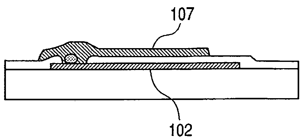
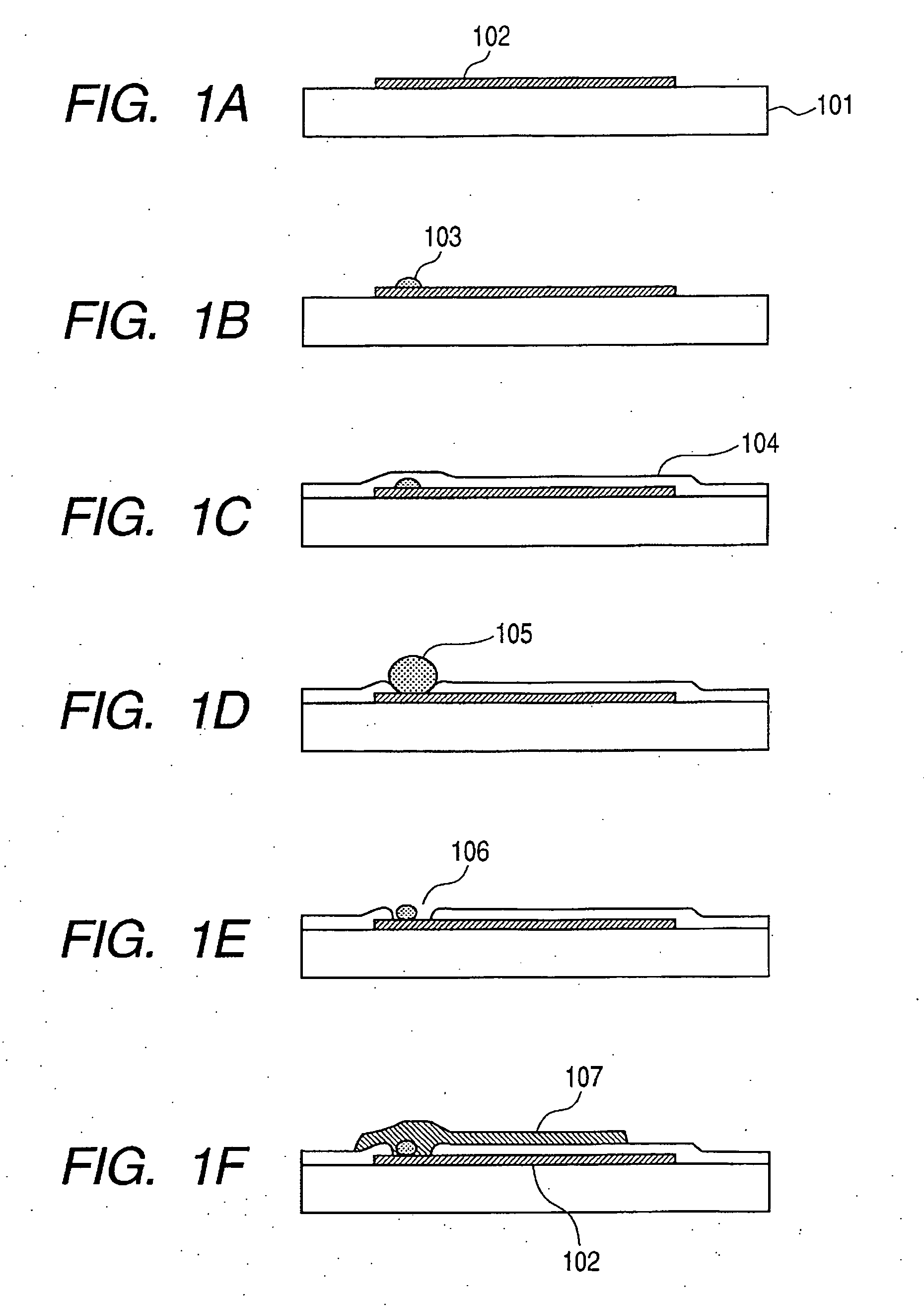
[0042] An example according to the present invention is described with reference to FIGS. 1A to 1F.
[0043] An aluminum thin film (aluminum wiring) 102 was deposited by vacuum deposition at the thickness of 3000 Å on a glass substrate 101. PVA (polyvinyl alcohol) 3% aqueous solution containing expandable resin particles (F-30VSD available from Matsumoto Yushi-Seiyaku Co., Ltd.) was printed on a desired position and dried to form the nucleus 103 having the diameter of about 30 μm. The diameter of the expandable particles before expansion was 3 to 7 μm.
[0044] Then, polyamic acid (SE812 available from NISSAN CHEMICAL INDUSTRIES, LTD.) 104 was applied so as to cover the nucleus, gradually heated, and baked at 250° C. for one hour to form a polyamide film. In the process of heating, the expandable resin became expanded particles 105 having the maximum particle diameter at 120° C., and a cleavage is formed in the polyamide film. Here, the maximum particle diameter of the expanded particle...
example 2
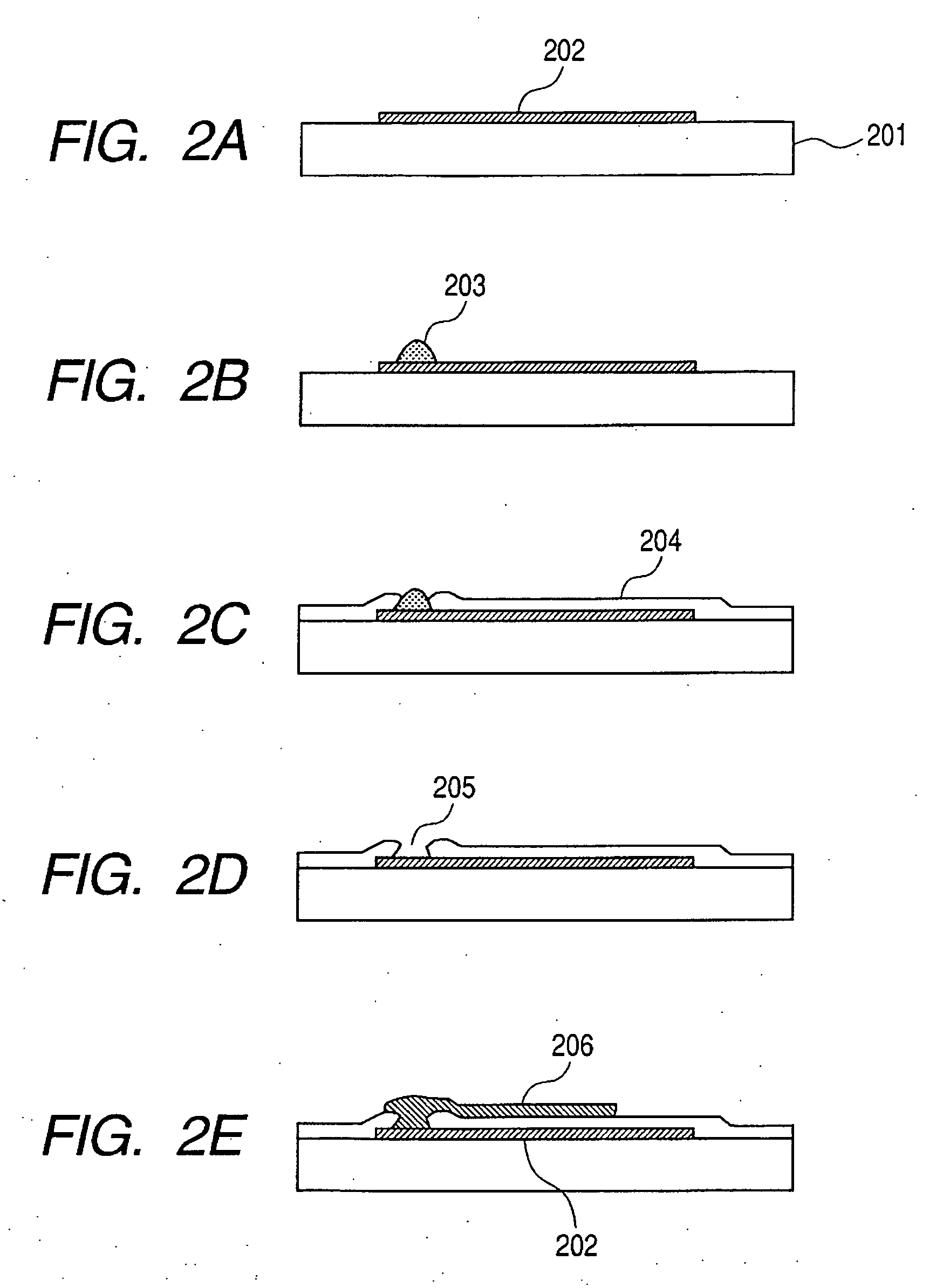
[0047] Another example according to the present invention is described with reference to FIGS. 2A to 2E.
[0048] Paraffin (1097-AH available from SAN NOPCO LTD.) was heated and, by using a manipulator equipped with a glass capillary, dropped to a desired position of a glass epoxy plate plated with copper at the thickness of 10 μm to form the nucleus 203 having the diameter of about 20 μm. A solution to be applied for forming an insulating film (Ceramate available from Catalysts & Chemicals Industries Co., Ltd.) 204 was spin-coated. The film was not formed at the position of the paraffin nucleus 203 and the paraffin nucleus was exposed. After prebaking at 100° C., the paraffin was removed with acetone to form the opening (contact hole) 205. Gold nanopaste (W101-20 available from Nippon Paint Co., Ltd.) was discharged into the opening using inkjet and baking was carried out at 300° C. for one hour to form the upper conductive layer (upper electrode) 206. Testing with a tester confirmed...
example 3
[0049] Still another example according to the present invention is described with reference to FIGS. 3A to 3E.
[0050] Gold nanopaste (W101-20 available from Nippon Paint Co., Ltd.) was discharged using inkjet to an alumina plate (substrate) 301 having a polished surface and baking was carried out at 300° C. for one hour to form the conductive layer (lower electrode) 302 in the thickness of 4000 Å. Silver paste having the viscosity of 10000 cP (DOTITE XA9069 available from FUJIKURA KASEI CO., LTD.) was dropped to a desired position of the conductive layer using a dispenser and baking was carried out at 150° C. for thirty minutes to form a nucleus 303 having the diameter of about 50 μm. Then, polyamic acid (SE812 available from NISSAN CHEMICAL INDUSTRIES, LTD.) 304 was applied so as to cover the nucleus, gradually heated, and baked at 250° C. for one hour to form a polyamide film. Here, a part of the lower conductive layer was masked such that the electrode could be taken out.
[0051] ...
PUM
| Property | Measurement | Unit |
|---|---|---|
| Electrical conductor | aaaaa | aaaaa |
| Electric field | aaaaa | aaaaa |
| aaaaa | aaaaa |
Abstract
Description
Claims
Application Information