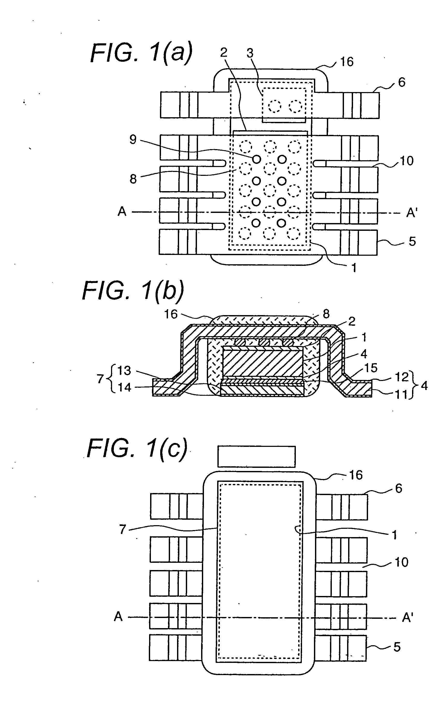
However, the
surface mounting type
package has a property that the fatigue strength of the bonding portion is weaker than that of the insert mounting type
package, because it has a structure in which the tip of the leads protruding from both sides of the resin body are bonded to the terminal of the substrate by
soldering two planes of small area to each other.
Therefore, it is necessary to absorb the
thermal strain between the package and the substrate resulting from
heat generation of the chip which causes deformation of the flexible leads.
In this case, a decrease of the electrical resistance of the
semiconductor package without a Si chip is difficult, because the electrical resistance of the lead itself is large.
However, if a position where the lead, to be connected to the electrode at an upper surface of the chip, protrudes from the resin body differs in height from the position where the die pad protrudes, the contacting planes of the upper and lower
metal molds for molding the resin form a three dimensional structure, such that a problem is created in that the manufacture of the
metal molds becomes difficult.
The above problem becomes significant when the
lead frame is a matrix frame (arranged in X and Y directions) and the objective is to manufacture a large number of the packages, simultaneously.
However, if the size of the die pad is the same as the size of the chip, the pressing portion can not be found on the die pad, and a problem is created in that the die pad is molded while being exposed at the bottom of the resin body.
Therefore, in case of a small size semiconductor package, wherein the size of the die pad is the same as the size of the chip, it is difficult to
assembly the structure in such a manner that the die pad concurrently operating as the
external connection terminals of the rear electrode is contained in the resin body.
However, currently, in view of environmental problems, no use of Pb is employed, and the conventional
soldering material containing Pb must be replaced with a new bonding material containing no Pb.
There are various
soldering materials containing no Pb having a
solidus line temperature below 250° C., but actually, there is no adequate soldering material containing no Pb having a
solidus line temperature higher than 270° C., which is durable against severe mounting on the substrate of the package.
The only exception is Au—Si solder having a
solidus line temperature of 370° C. However, Au—Si solder can not be adopted as the soldering material for the electrode at the rear plane of the chip, for two reasons, such as high cost and generation of cracks in the chip during the cooling step after soldering when the size of the chip is large, because of the high yield strength.
Therefore, a problem exists in that there is no soldering material containing no Pb to replace the soldering material containing Pb.
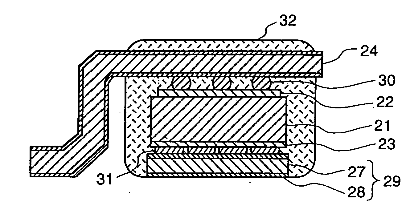
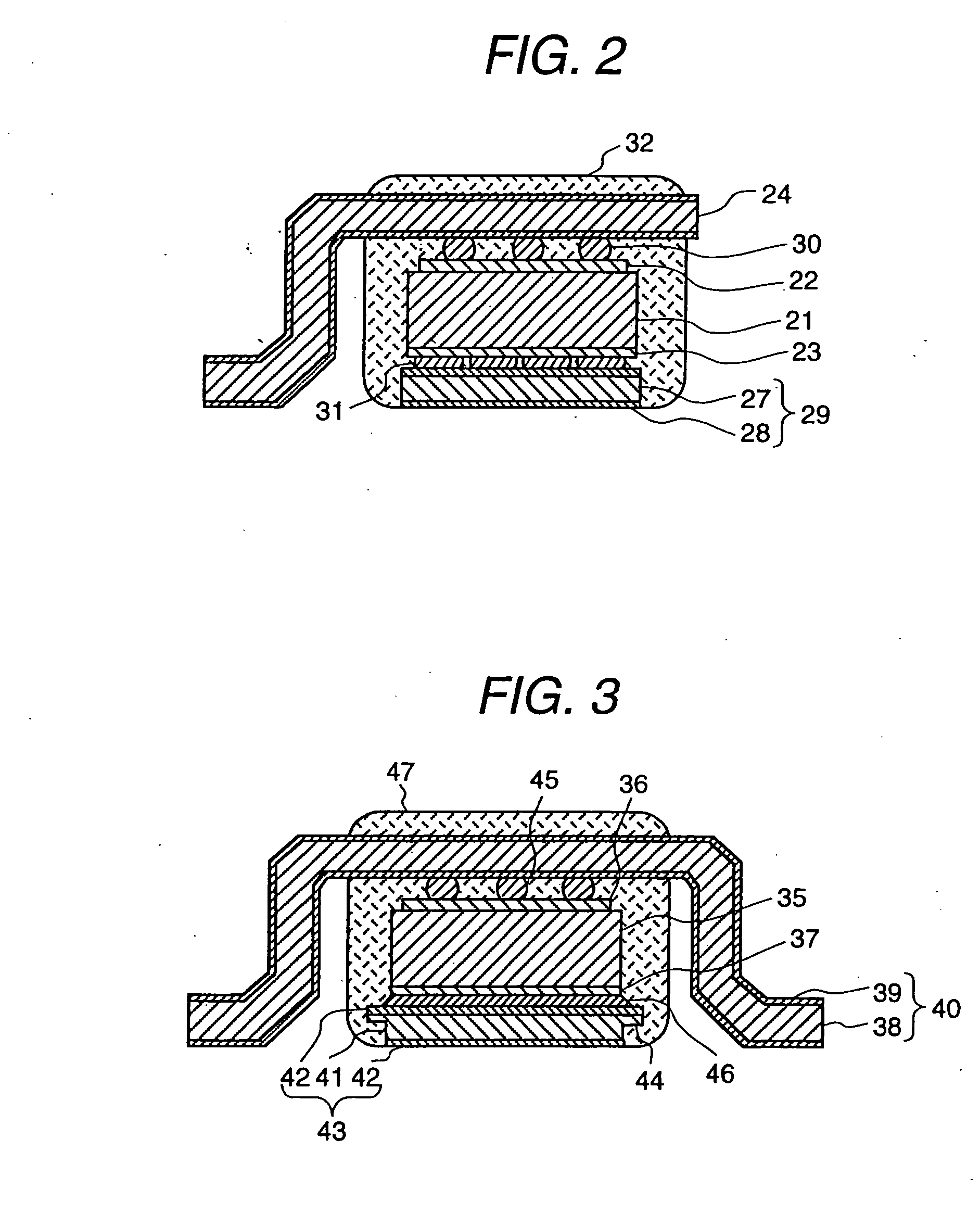
On the other hand, adhesion with a resin with conductive particles is durable thermally in a short time against the necessary temperature for the mounting , i.e. 270° C., but is weak in
mechanical strength, because the
adhesion strength is maintained by the resin.
Even though tightness of the adhesion is reinforced with a shrinking force by curing the molding resin, a package having a large area or a package used in a high temperature has a problem in that the electric resistance and
thermal resistance at the bonding portion are increased in accordance with deterioration of the resin, which is caused by a change with elapsing time or temperature cycles.
In particular, because the one plane molding structure, wherein the die pad (
external connection terminals) is exposed to the surface of the resin body, is a structure which can not receive sufficient pressing force from the molding resin at the rear plane of the chip, a problem is raised in that the long term reliability of the resin using conductive particles for adhesion is further decreased.

