Method of stabilizing film quality of low-dielectric constant film

a low-dielectric constant and film quality technology, applied in the field of manufacturing semiconductor devices, can solve the problems of reducing the mechanical strength of the film, unable to achieve satisfactory improvement of plasma fluctuation and unstable state, and difficulty in forming a low-dielectric constant film having stable film quality without plasma damag

Active Publication Date: 2006-09-28
ASM JAPAN
View PDF11 Cites 5 Cited by
  • Summary
  • Abstract
  • Description
  • Claims
  • Application Information

AI Technical Summary

Benefits of technology

[0010] As a dielectric constant is lowered along with accelerated progress in ultrafine semiconductor devices, mechanical strength of a film decreases, and because of this, problems related to integration and packaging occur. In order to bring improvement in these problems, in view of the time required, setting out of peripheral process conditions, etc., it is inclined to select relatively high dielectric constants for the 65-90 nm generation. Additionally, in order to lower a dielectric constant, there is the need for reducing a thickness of an interlayer insulation film on a wiring for which a low dielectric constant (low-k) film is used.
[0011] In an embodiment of the present invention, in consideration of these problems in the conventional techniques, one of the objects is to form a low dielectric constant film with controlled plasma damage and stable film quality. Additionally, in an embodiment, one of the objects is to form a low dielectric constant film having high mechanical strength stably. Further, in an embodiment, one of the objects is to provide an apparatus for accomplishing the above-mentioned objects. Additionally, in an embodiment, one of the objects is to provide a method of stabilizing a plasma inside a reactor.

Problems solved by technology

Using these conventional techniques, however, it is difficult to form a low dielectric constant film having stable film quality without plasma damage.
It is thought that one of the causes for this is that these conventional techniques have not satisfactorily accomplished improvement of plasma fluctuation and unstable state.
As a dielectric constant is lowered along with accelerated progress in ultrafine semiconductor devices, mechanical strength of a film decreases, and because of this, problems related to integration and packaging occur.

Method used


Image

  • Method of stabilizing film quality of low-dielectric constant film
  • Method of stabilizing film quality of low-dielectric constant film
  • Method of stabilizing film quality of low-dielectric constant film

Examples


example 1

A State Before the Improvement

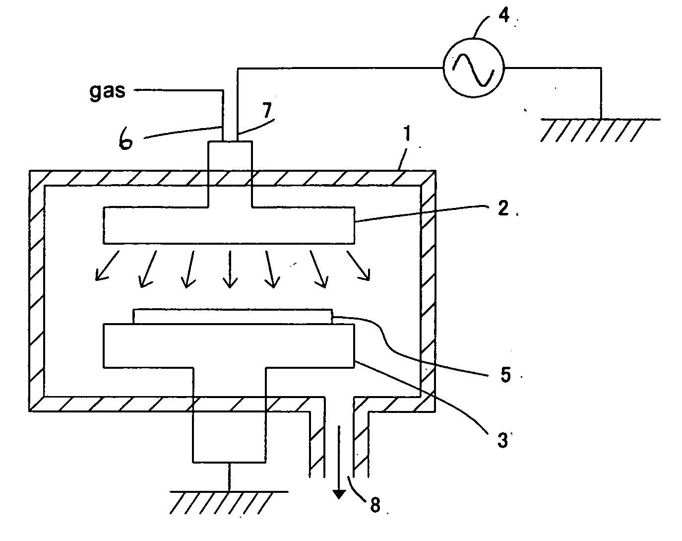
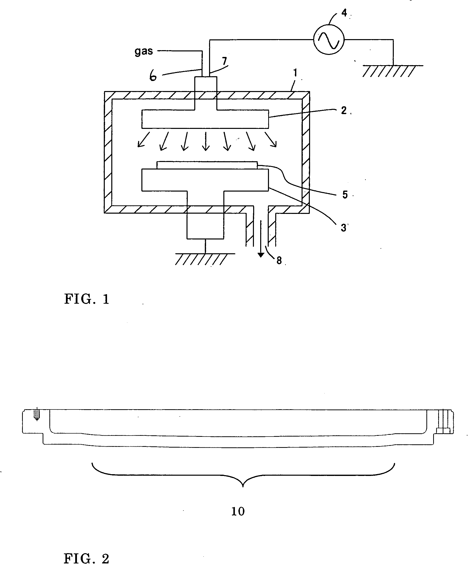
[0071] Workpiece: Low-k silicon insulation film [0072] Upper electrode: Flat [0073] Lower electrode: Flat (The entire surface is in contact.) [0074] DM-DMOS: 200 sccm [0075] He: 140 sccm [0076] Isopropyl alcohol: 400 sccm [0077] O2: 200 sccm [0078] Pressure: 800 Pa [0079] Heat treatment temperature: 380° C. [0080] Deposition growth rate: 800 nm / min [0081] Dielectric constant: 2.6 [0082] Hardness: 1.0 GPa [0083] Modulus: 6 GPa [0084] Antenna TEG yield: 60%

example 2

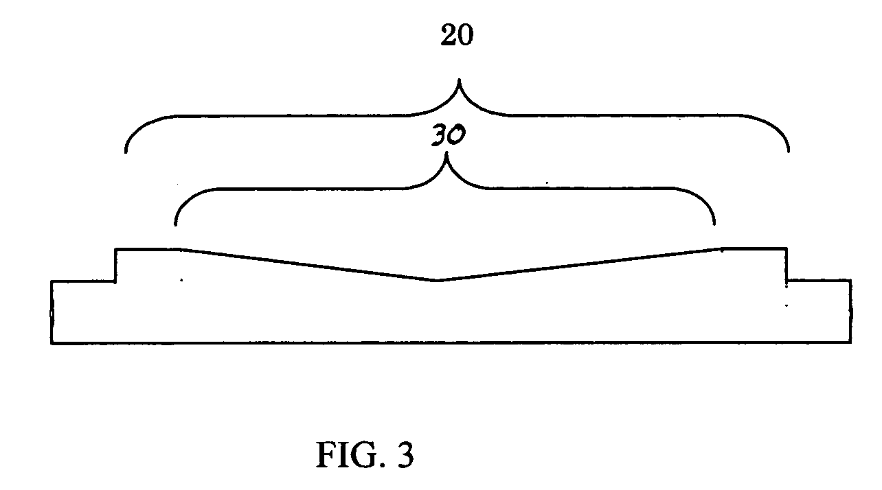
[0085] Workpiece: Low-k silicon insulation film [0086] Upper electrode: 1 mm convex type [0087] Lower electrode: 0.5mm concave type [0088] DM-DMOS: 200 sccm [0089] He: 140 sccm [0090] Isopropyl alcohol: 400 sccm [0091] O2: 200 sccm [0092] Pressure: 800 Pa [0093] Heat treatment temperature: 380° C. [0094] Deposition growth rate: 790 nm / min [0095] Dielectric constant: 2.6 [0096] Hardness: 1.0 GPa [0097] Modulus: 6 GPa [0098] Antenna TEG yield: 80%

example 3

[0099] Workpiece: Low-k silicon insulation film [0100] Upper electrode: 3.0 mm convex type [0101] Lower electrode: 0.5 mm concave type [0102] DM-DMOS: 200 sccm [0103] He: 140 sccm [0104] Isopropyl alcohol: 400 sccm [0105] O2: 100 sccm [0106] Pressure: 600 Pa [0107] Heat treatment temperature: 380° C. [0108] Dielectric constant: 2.62 [0109] Deposition growth rate: 750 nm / min [0110] Hardness: 1.1 GPa [0111] Modulus: 7 GPa [0112] Antenna TEG yield: 100%


PUM

PropertyMeasurementUnit
temperatureaaaaaaaaaa
dielectric constantsaaaaaaaaaa
leakage current distributionaaaaaaaaaa

Abstract

A method of forming a film having a low dielectric constant, comprises the steps of: placing a substrate between an upper electrode and a lower electrode inside a reaction chamber, introducing a silicon-containing hydrocarbon compound source gas, an additive gas, and an inert gas into a space between the upper and lower electrodes by controlling a gas flow ratio, generating a plasma by applying RF power to the space between the upper and lower electrodes in a state in which an interval between the upper electrode and the substrate is narrower in the vicinity of a center of the substrate than that in the vicinity of its periphery, and forming a film having a low dielectric constant on the substrate at a deposition rate of less than approx. 790 nm / min by controlling a flow rate of the process gas.

Description

BACKGROUND OF THE INVENTION [0001] 1. Field of the Invention [0002] The present invention relates to manufacturing semiconductor devices; particularly to a method of forming a low dielectric constant film having improved film strength by inhibiting plasma damage, using plasma CVD. [0003] 2. Description of the Related Art [0004] Film formation on a semiconductor substrate by plasma chemical vapor deposition (a plasma CVD method) is carried out by placing a semiconductor substrate, which is a workpiece, on a resistance-heating type heater a temperature of which is raised to 50-550° C., in 1-10 Torr atmosphere. By disposing the heater by pairing with a shower-plate jetting out a reaction gas, a plasma is generated by radio-frequency discharge between the heater and the shower-plate by applying radio-frequency power at 13.56-60 MHz at an output of 100-4,000 W to the shower-plate. [0005] Using plasma CVD methods, thin film formation of interlayer insulation films, passivation films, refl...

Claims


Application Information

Patent Timeline
Patent Type & Authority Applications(United States)
IPC IPC(8): H05H1/24C23C16/00
CPCC23C16/30C23C16/5096H01J37/32082H01L21/02126H01L21/02216H01L21/02274H01L21/3122H01L21/31633
Inventor FUKAZAWA, ATSUKIITOH, KIYOTOKIMURA, TSUNAYUKIMATSUKI, NOBUO
Owner ASM JAPAN
Why Eureka
Try Eureka