
Metal-insulator-metal (MIM) capacitor structure and methods of fabricating same

a technology of metal-insulator metal and capacitors, which is applied in the direction of capacitors, semiconductor devices, semiconductor/solid-state device details, etc., can solve the problems of inordinate oxidation of the bottom electrode during fabrication, limited design of capacitors providing the necessary capacitance for many applications (e.g., many rf applications), and achieve the effect of improving the overall capacitance density

Inactive Publication Date: 2006-09-28
NXP BV
View PDF8 Cites 7 Cited by
  • Summary
  • Abstract
  • Description
  • Claims
  • Application Information

AI Technical Summary

Benefits of technology

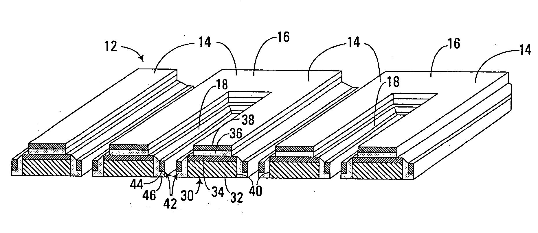
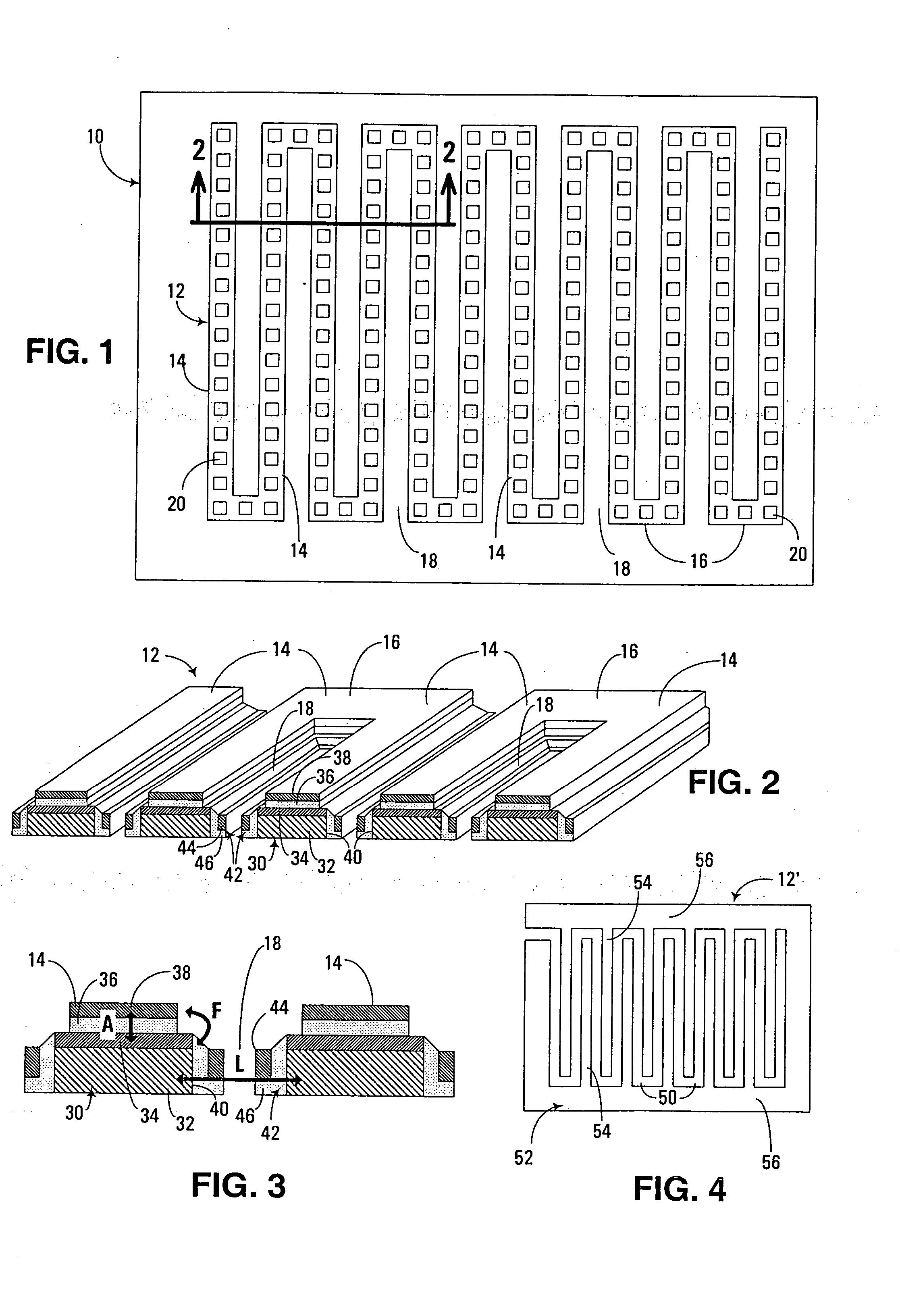
[0016] The invention addresses these and other problems associated with the prior art by providing in one aspect a Metal-Insulator-Metal (MIM) capacitor structure and method of fabricating the same in an integrated circuit in which a sidewall spacer extends along a channel defined between a pair of legs that define portions of the MIM capacitor structure. Each of the legs includes top and bottom electrodes and an insulator layer interposed therebetween, as well as a sidewall that faces the channel. The sidewall spacer incorporates a conductive layer and an insulator layer interposed between the conductive layer and the sidewall of one of the legs, and the conductive layer of the sidewall spacer is physically separated from the top electrode of the MIM capacitor structure. By orienting a sidewall spacer, with a conductive layer that is physically separated from a top electrode, along the channel, it has been found that lateral capacitance effects between the pair of legs that face the channel are substantially increased, resulting in substantial improvements in overall capacitance density for the MIM capacitor structure.
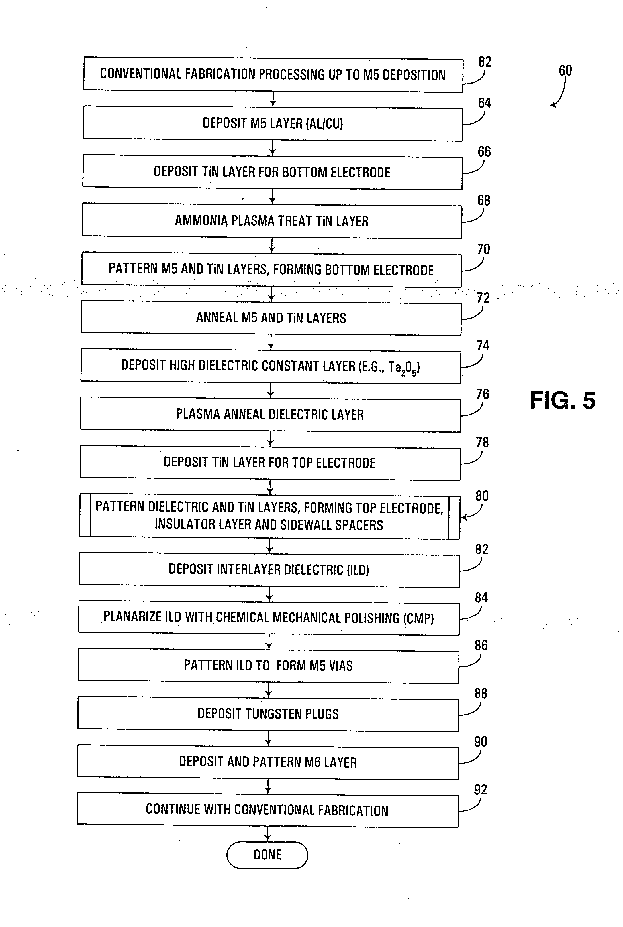
[0018] The invention also addresses in another aspect a number of improvements to the process of making MIM capacitor structures. For example, one aspect of the invention addresses the difficulties associated with oxidation of the bottom electrode of a MIM capacitor structure by providing a MIM capacitor structure and method of fabricating the same in an integrated circuit in which a surface of the bottom electrode is ammonia plasma treated. As another example, another aspect of the invention addresses the difficulties associated with the exposure of aluminum interconnects to etching chemistry, by utilizing a multi-rate etching process to etch the top electrode and insulator layer of an MIM structure, using a first, higher rate to perform an anisotropic etch up to a point proximate an interface between the conductive and dielectric materials respectively defining the top electrode and insulator layer of the MIM structure, and then using a second, lower rate to perform an anisotropic etch to a point proximate an etch stop layer defined on the bottom electrode of the MIM structure. Through the use of an etch stop layer, underlying aluminum interconnects are protected from undue exposure to etching chemistry, thus eliminating in many instances the need for the aluminum polymer removal and related cleaning processes.

Problems solved by technology

Nonetheless, despite the improvements made in conventional MIM capacitor designs, many such designs are limited to at most about 1 fF / μm2.
At this density, however, capacitors providing the necessary capacitance for many applications (e.g., many RF applications) are inordinately large, particularly for more advanced design rules.
Another difficulty experienced in connection with MIM capacitor fabrication is oxidation of the bottom electrode during fabrication.
Particularly when electrode materials such as titanium nitride (TiN) are used, oxidation of the electrode prior to deposition of the insulator layer can occur and form titanium oxides that cause current leakage.
Furthermore, close coupling of the bottom electrode and dielectric film depositions does not guarantee a clean interface between the materials.
Yet another difficulty experienced in connection with MIM capacitor fabrication is that of patterning and etching the MIM capacitor structure in connection with aluminum-based circuit interconnects.
Adding such a step increases processing time and expense, and may not remove all chlorine (Cl) containing compounds that can cause Al corrosion.

Method used


Image

  • Metal-insulator-metal (MIM) capacitor structure and methods of fabricating same
  • Metal-insulator-metal (MIM) capacitor structure and methods of fabricating same
  • Metal-insulator-metal (MIM) capacitor structure and methods of fabricating same

Examples


working examples

Ammonia Plasma Treatment

[0088] As discussed above, an ammonia plasma treatment may be introduced to prevent oxidation of a TiN lower electrode after M5 deposition. The process described above was tested by processing bare silicon 200-mm test wafers with different treatment times. A thin silicon nitride film was measured after the ammonia treatment. FIG. 8 illustrates the resulting silicon nitride growth on the test wafers.

[0089] The data was taken from a 49-point measurement with a 3 mm edge exclusion measured by an Optiprobe model 5240, a tool available from Therma-wave Corporation that uses spectral ellipsometry and fine angle reflectometry to measure stacks of thin transparent films. The 180 second treatment time was noted as providing an acceptable compromise between processing time and the uniformity of silicon nitride.

[0090] Ammonia plasma treatment was also found to alter voltage linearity. For test samples constructed using the aforementioned process, when varying the vo...


PUM


Abstract

A Metal-Insulator-Metal (MIM) capacitor structure and method of fabricating the same in an integrated circuit improve capacitance density in a MIM capacitor structure by utilizing a sidewall spacer extending along a channel defined between a pair of legs that define portions of the MIM capacitor structure. Each of the legs includes top and bottom electrodes and an insulator layer interposed therebetween, as well as a sidewall that faces the channel. The sidewall spacer incorporates a conductive layer and an insulator layer interposed between the conductive layer and the sidewall of one of the legs, and the conductive layer of the sidewall spacer is physically separated from the top electrode of the MIM capacitor structure. In addition, the bottom electrode of a MIM capacitor structure may be ammonia plasma treated prior to deposition of an insulator layer thereover to reduce oxidation of the electrode. Furthermore, a multi-rate etching process may be used to etch the top electrode and insulator layer of an MIM structure, using a first, higher rate to perform an anisotropic etch up to a point proximate an interface between the conductive and dielectric materials respectively defining the top electrode and insulator layer of the MIM structure, and then using a second, lower rate to perform an anisotropic etch to a point proximate an etch stop layer defined on the bottom electrode of the MIM structure.

Description

FIELD OF THE INVENTION [0001] The invention is generally related to integrated circuit fabrication, and more particularly, to the fabrication of metal-insulator-metal (MIM) capacitor structures in integrated circuits. BACKGROUND OF THE INVENTION [0002] Reduced circuit area is an economic driver of the microelectronics revolution. Integrated circuits, or chips, continue to increase in circuit density due to reduced sizes of circuit components made possible through the implementation of smaller and smaller circuit design rules. As more and more components are designed into an integrated circuit, the complexity of the integrated circuit is increased, thereby enabling greater functionality in the circuit. Moreover, functions that were once performed by multiple integrated circuits can often be integrated together onto the same integrated circuit, thereby reducing costs, power consumption, and size, while improving speed and interconnectivity. [0003] In addition, other components such as...

Claims


Application Information

Patent Timeline
Patent Type & Authority Applications(United States)
IPC IPC(8): H01L21/20H01L21/02H01L21/822H01L27/04
CPCH01L21/76834H01L21/76852H01L23/5223H01L27/016H01L2924/0002H01L28/60H01L2924/00H10B99/00
Inventor OLEWINE, MICHAELSAIZ, KEVIN
Owner NXP BV
Learn More