Integrated optical metrology and lithographic process track for dynamic critical dimension control

a dynamic critical dimension control and optical metrology technology, applied in the field of lithographic processes, can solve the problems of increasing the level of cd error, increasing the accuracy and resolution requirements of lithographic patterning process, and continuing evolution toward smaller device size and higher density, so as to improve the yield and throughput of a lithographic process track

Inactive Publication Date: 2006-10-05
TAIWAN SEMICON MFG CO LTD
View PDF7 Cites 26 Cited by
  • Summary
  • Abstract
  • Description
  • Claims
  • Application Information

AI Technical Summary

Benefits of technology

[0009] To achieve the foregoing and other objects, and in accordance with the purposes of the present invention, as embodied and broadly de

Problems solved by technology

One of the limiting factors in the continuing evolution toward smaller device size and higher density has been the increasingly stringent requirements placed on the accuracy and resolution of lithographic patterning processes.
As semiconductor device CD's are scaled down to below about 100 nm, small nanometer sized variations in a resist profile make up an increasingly larger percentage of the CD, thereby increasing the level of CD error.
Nonuniform resist patterning may adversely affect the manufacturing process as well as the reliability of integrated circuits in several ways.
For example, unacceptable within-wafer CD variations require that the lithographic process be repeated, which lowers wafer throughput and increases production costs.
For example SEM processes obtain surface CD information, but are not able to obtain profiles of developed resist patterns.
TEM, on the other hand, requires time c

Method used


Image

  • Integrated optical metrology and lithographic process track for dynamic critical dimension control
  • Integrated optical metrology and lithographic process track for dynamic critical dimension control
  • Integrated optical metrology and lithographic process track for dynamic critical dimension control

Examples


Embodiment Construction

[0019] Although the system and method of the present invention are explained in exemplary implementation with respect to achieving CD accuracy and uniformity of a patterned resist layer in an integrated circuit manufacturing process, it will be appreciated that the invention may be adapted for application to micro-engineered machine (MEM) processes or other processes where resist patterns with critical dimensions (CD's) of less than about 0.25 microns are formed for subsequent dry etching according to the patterned resist layer.

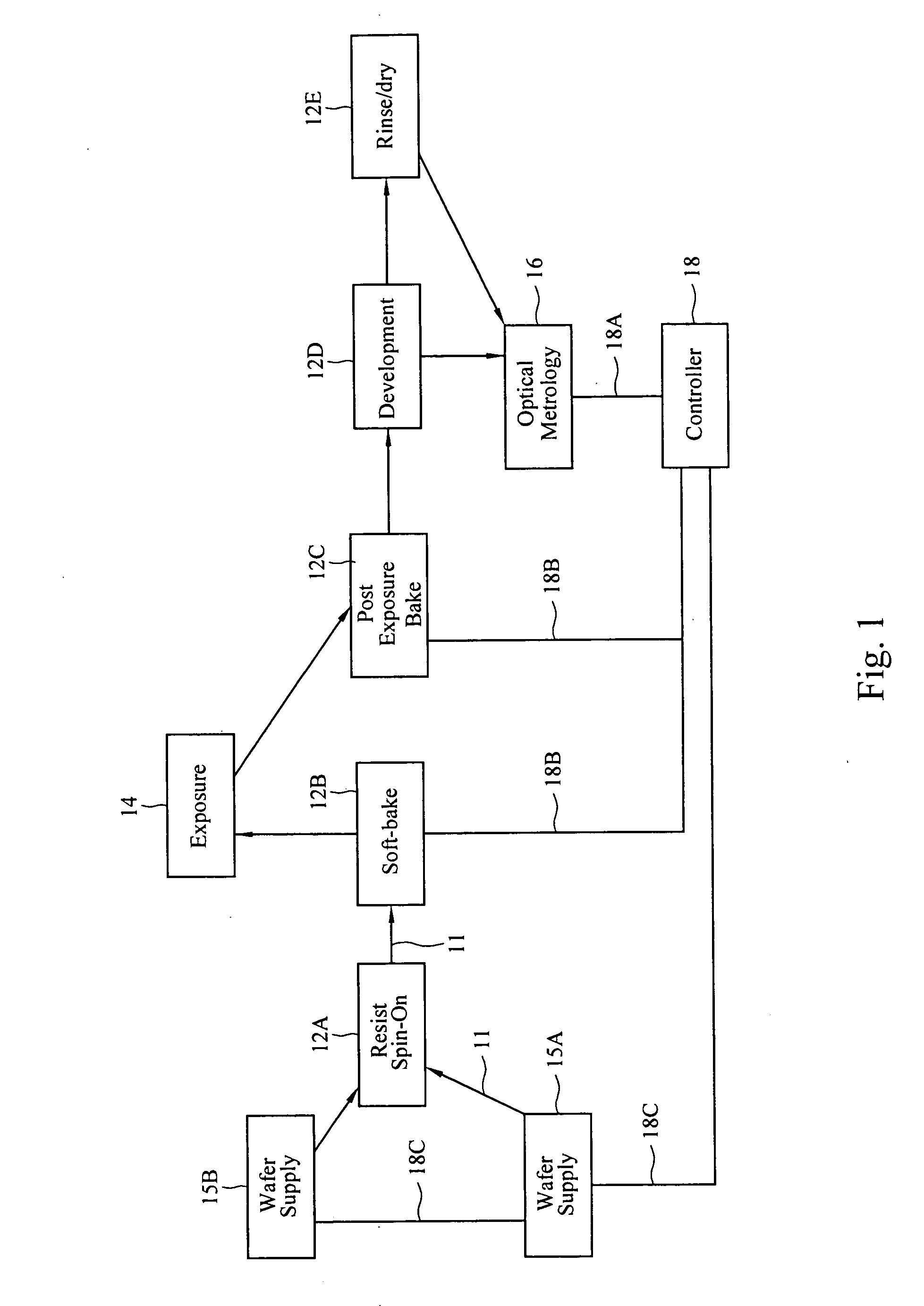
[0020] Referring to FIG. 1, in an exemplary implementation of the present invention, an exemplary lithography process track is schematically represented, showing a conventional resist spin-on station 12A, a soft-bake station 12B, a post exposure bake (PEB) station 12C, a development station 12D, and a rinse / dry station 12E. Arrows e.g., 11 indicate an exemplary process flow on the lithography process track including transfer to an exposure station 14 e.g., s...


PUM


Abstract

A method and apparatus for improving a yield and throughput of a lithographic process track, the method including providing a first resist layer on a first process wafer; forming a first resist pattern in the first resist layer including a heating process according to a first temperature profile wherein the heating process comprises a plurality of temperature controllable heating zones; producing and collecting scattered light spectra from the first resist pattern processing the scattered light spectrum to obtain 3-dimensional information including first resist pattern critical dimensions; determining a second temperature profile for performing the heating process to achieve targeted resist pattern critical dimensions including a second resist pattern on a second process wafer; and, forming the second resist pattern dimensions including the heating process according to the second temperature profile.

Description

FIELD OF THE INVENTION [0001] This invention generally relates to lithographic processes and more particularly to resist baking and development processes in an integrated circuit manufacturing process including an integrated temperature control and optical metrology system for achieving dynamic and real-time adjustments in a resist baking process to achieve improved critical dimension (CD) and critical dimension uniformity (CDU) control in a lithography process including increased wafer throughput. BACKGROUND OF THE INVENTION [0002] Since the introduction of semiconductor devices, the size of semiconductor devices has been continuously shrinking, resulting in smaller semiconductor chip size and increased device density. One of the limiting factors in the continuing evolution toward smaller device size and higher density has been the increasingly stringent requirements placed on the accuracy and resolution of lithographic patterning processes. Various methods have been implemented to...

Claims


Application Information

Patent Timeline
IPC IPC(8): G03B27/00G03C5/00
CPCG03F7/70625A47J27/0802A47J27/09A47J36/06
Inventor KE, CHIH-MINGYU, SHING-SHENWANG, YU-HSIGAU, TSAI-SHENGHUANG, JACKY
Owner TAIWAN SEMICON MFG CO LTD
Why Eureka
Try Eureka