Electronic device substrate and its fabrication method, and electronic device and its fabrication method

Inactive Publication Date: 2006-10-12
HITACHI CABLE +1
View PDF12 Cites 66 Cited by
  • Summary
  • Abstract
  • Description
  • Claims
  • Application Information

AI Technical Summary

Benefits of technology

[0074] According to the present invention, in the electronic device substrate and the electronic device, it is possible to reduce device size without applying stress to a package, as the core substrate is released from the electronic device substrate side with

Problems solved by technology

According to the conventional electronic device, in the configuration of FIG. 4, however, there is the problem with very poor adhesion of the gold plating in the functional plating 23 to sealing resin 10.
Specifically, when gold plating is applied to the surface of the functional plating 23, the gold does not form a high electronegativity oxide film, which results in poor adhesion to the sealing resin, and degrades reliability of the electronic device.
However, even this method cannot entirely avoid the following:
To avoid this failure, JP-A-2002-9196 also describes a method thickening the metal of the wiring pattern and fabrication on a periphery an overhanging portion that slightly projects on its sealing resin side, but because the thickn

Method used


Image

  • Electronic device substrate and its fabrication method, and electronic device and its fabrication method
  • Electronic device substrate and its fabrication method, and electronic device and its fabrication method
  • Electronic device substrate and its fabrication method, and electronic device and its fabrication method

Examples


first embodiment

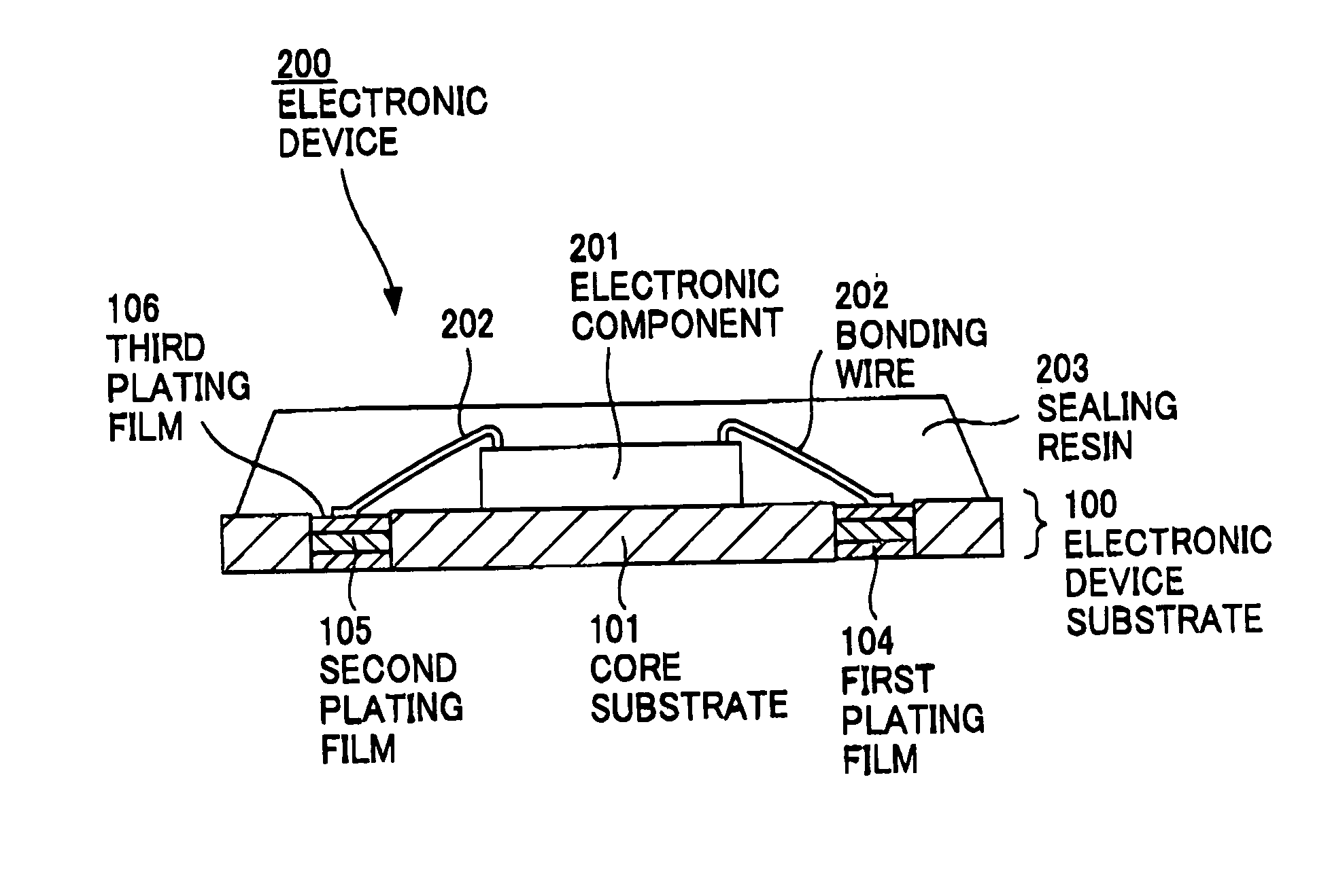
[0094]FIG. 5 shows an electronic device substrate according to the present invention. This electronic device substrate 100 comprises a core substrate 101 formed of copper foil as base material, a photo solder resist (hereinafter, “PSR”) film 102 as a first electrical insulation layer formed in a specified pattern on the core substrate 101, a first plating film 104 provided in an opening 103 formed in a specified position of the PSR film 102, a second plating film 105 provided on the first plating film 104, and a third plating film 106 provided on the second plating film 105.

[0095] From the points of view of availability, cost, high electrical conductivity, and removability in a final step, the core substrate 101 most preferably comprises copper foil, but may comprise stainless foil, aluminum or aluminum alloy foil, nickel or nickel alloy foil, tin or tin alloy foil.

[0096] The core substrate 101 needs to be 20 μm or more thick because mechanical durability is required in carrying an...

second embodiment

[0114] Next, there will be explained a fabrication method of the electronic device of FIG. 7 according to the FIGS. 8A-8E show a fabrication method of the electronic device of FIG. 7.

[0115] There is first prepared an electronic device substrate 100 as shown in FIG. 8A. Next, as shown in FIG. 8B, after an electronic component (IC chip) 201 having an aluminum electrode terminal not shown on a top surface is bonded with a die bonding paste to a coated surface of the PSR film 102 of the electronic device substrate 100, the aluminum electrode terminal of electronic component 201 and the third plating film 106 are electrically connected to each other with metallic bonding wires 202, as shown in FIG. 8C.

[0116] Next, this is followed by sealing resin 203 sealing for covering the electronic component 201, bonding wires 202, and third plating film 106 for protecting the electronic component 201 and bonded portions from external environment, as shown in FIG. 8D.

[0117] Next, a ferric chlorid...

third embodiment

[0128] Next, there will be explained a fabrication method of the electronic device substrate according to the FIGS. 10A-10G show a fabrication method of the electronic device substrate 100 of FIG. 9.

[0129] First, a carrier-laminated core substrate 120 (FIG. 10A) is coated with a 15 μm thick PSR film 102 by screen printing, as shown in FIG. 10B. Next, as shown in FIG. 10C, using a photomask 108, the PSR film 102 is irradiated with ultraviolet rays 107 via the photomask 108. As shown in FIG. 10D, this is followed by development and formation of openings 103 in a desired shape on the PSR film 102.

[0130] Next, as shown in FIG. 10E, the surface of the carrier layer 121 is protected with a plating-resistant chemical electrical insulation tape (masking tape) 109, followed by immersion in an electrical gold plating liquid for forming a first plating film 104 and, using the core substrate 120 as a cathode, a 0.5 μm thick gold plating film is applied to the opening as a first plating film 1...


PUM

PropertyMeasurementUnit
Lengthaaaaaaaaaa
Lengthaaaaaaaaaa
Thicknessaaaaaaaaaa

Abstract

An electronic device substrate is provided with a thin-plate core substrate; a metal electrode provided on the core substrate and electrically connected to an electrode of an electronic component to be packaged thereon; and an electrical insulation layer on which is mounted the electronic component, and which is provided to surround the metal electrode.

Description

[0001] The present application is based on Japanese patent application Nos. 2005-76674 and 2005-290463, the entire contents of which are incorporated herein by reference. BACKGROUND OF THE INVENTION [0002] 1. Field of the Invention [0003] The present invention relates to an electronic device substrate and its fabrication method, and an electronic device and its fabrication method. Particularly, it relates to an electronic device substrate and its fabrication method, and an electronic device and its fabrication method, which is capable of releasing a core substrate from an electronic device substrate side with weak force, reducing the load of chemical or electrochemical dissolution, or mechanical grinding for exposing a terminal surface to a lower surface, and reducing size. [0004] 2. Description of the Related Art [0005]FIGS. 1A and 1B are respectively a front cross-sectional view and a plan view showing an electronic component mount surface of a conventional electronic device. This...

Claims


Application Information

Patent Timeline
IPC IPC(8): H05K7/00H05K3/30
CPCH01L21/486Y10T29/49146H01L21/6835H01L23/3121H01L23/49827H01L2221/68345H01L2224/48227H01L2224/48247H01L2224/85001H01L2924/01046H01L2924/01078H01L2924/01079H01L2924/15173H01L2924/15311H01L2924/19041H01L24/48H01L2924/01019H01L2924/01067H01L2224/45144H01L21/568Y10T29/49139Y10T29/49124Y10T29/49126H01L2924/1461Y10T29/49155Y10T29/4913Y10T29/49165H01L2924/00H01L2224/451H01L2924/00014H01L24/45H01L2924/14H01L2924/181H01L2224/05554H01L2924/10161H01L24/49H01L2224/49171H01L2224/05599H01L2924/00012A47L15/4217A47L2501/01
Inventor CHINDA, AKIRAMIYAMOTO, NOBUAKIHIRASAWA, KOKIUCHIDA, KENJIMITA, MAMORU
Owner HITACHI CABLE
Why Eureka
Try Eureka