Light emitting device
a technology of light emitting device and discharge tube, which is applied in the direction of discharge tube/lamp details, discharge tube luminescnet screen, electric discharge lamp, etc., can solve the problems of high contact resistance easy oxidation of aluminum or silver, and increase of drive voltag
- Summary
- Abstract
- Description
- Claims
- Application Information
AI Technical Summary
Benefits of technology
Problems solved by technology
Method used
Image

Examples
embodiment mode 1
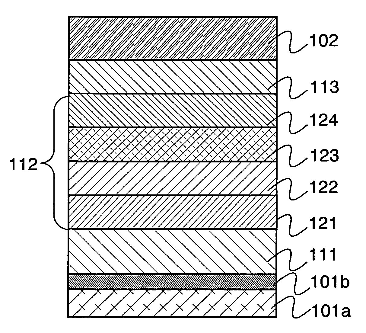
[0043] In this embodiment mode, a structure of a light-emitting element will be explained.
[0044] As shown in FIG. 1, a light-emitting element according to the present invention has a first electrode 101 and a second electrode 102 which oppose to each other, and a first layer 111, a second layer 112, and a third layer 113 are sequentially stacked over the first electrode 101. Such a light-emitting element can emit light when there is potential difference between the first electrode 101 and the second electrode 102. For example, when the first electrode has higher potential than that of the second electrode, holes are injected from the first layer 111 to the second layer 112 and electrons are injected from the third layer 113 to the second layer 112. The holes and the electrons are recombined in the second layer 112 and light-emitting substances are excited. Then, the excited light-emitting substances emit light in returning to a ground state; thus, light emission can be obtained fro...
embodiment mode 2
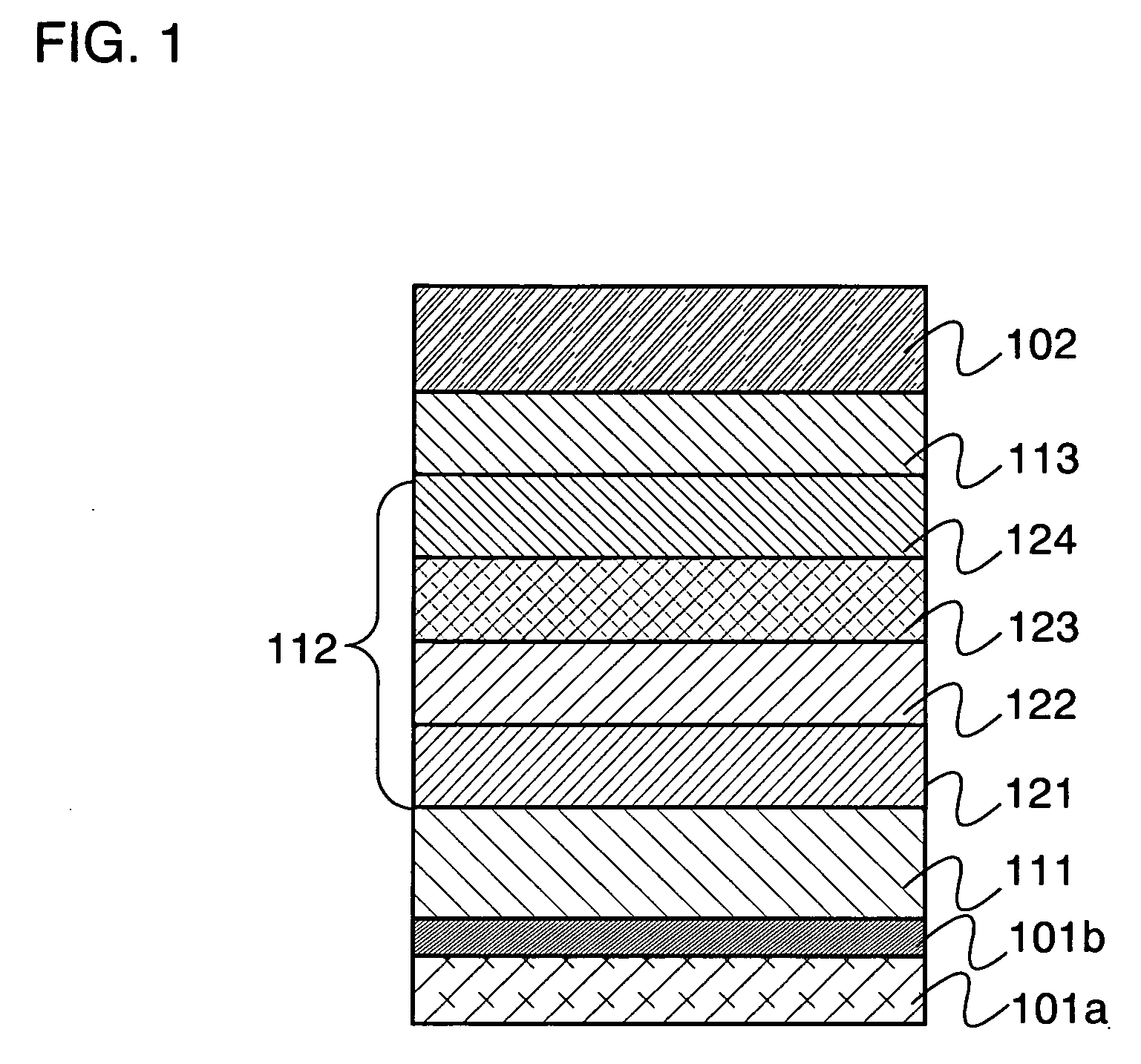
[0079] Further, according to the present invention, a film thickness of any one of layer in an electroluminescent layer may be differed depending on a light-emitting element in which each light-emission color (red, green, and blue) is emitted. Consequently, light extraction efficiency of a light-emitting element the emission wavelength of which differs can be increased. In this embodiment mode, in addition to the electrode structure shown in Embodiment Mode 1, a light-emitting element in which a film thickness of any one of layer in an electroluminescent layer, in other words, layers except a first electrode and a second electrode will be explained.
[0080] As shown in FIG. 2, light-emitting elements that emit light of red (R), green (G) and blue (B) share the film thickness of a first electrode 101 having reflectiveness and a second electrode 102 having a light-transmitting property, and further the film thickness of any one of first layers 111R, 111G and 111B, second layers 112R, 1...
embodiment mode 3
[0089] In this embodiment mode, a cross-sectional structure of a pixel included in a light-emitting element according to the present invention will be explained. In addition, a transistor for controlling current supplied to a light-emitting element (hereinafter, referred to as a driving transistor) is to be a p-type thin film transistor (TFT).
[0090]FIG. 3 is a cross-sectional view, which shows a so-called top emission type in which light emitted from each of light-emitting elements 603R, 603G, and 603B is extracted through a second electrode 102. In addition, each light-emission color (RGB) can be emitted from the light-emitting elements 603R, 603G, and 603B, respectively (hereinafter, referred to as a light-emitting element 603 together). The light-emitting elements 603 each have a stacked first electrode 101 (including a first conductive layer 101a and a second conductive layer 101b) and the second electrode 102, and electroluminescent layers 605R, 605G, and 605B are provided the...
PUM
 Abstract
Description
Claims
Application Information
 - Generate Ideas
- Intellectual Property
- Life Sciences
- Materials
- Tech Scout
- Unparalleled Data Quality
- Higher Quality Content
- 60% Fewer Hallucinations
Browse by: Latest US Patents, China's latest patents, Technical Efficacy Thesaurus, Application Domain, Technology Topic, Popular Technical Reports.
© 2025 PatSnap. All rights reserved.Legal|Privacy policy|Modern Slavery Act Transparency Statement|Sitemap|About US| Contact US: help@patsnap.com