Semiconductor laser device, method for manufacturing the same, and optical pickup device using the same

a laser device and semiconductor technology, applied in semiconductor lasers, laser cooling arrangements, laser details, etc., can solve the problems of increasing the operating current value, reducing the efficiency of the semiconductor laser device, and a high leakage current, so as to reduce the density of carriers injected into the rear facet portion of the active layer, the effect of high reliability

Inactive Publication Date: 2006-10-19
PANASONIC CORP
View PDF6 Cites 7 Cited by
  • Summary
  • Abstract
  • Description
  • Claims
  • Application Information

AI Technical Summary

Benefits of technology

[0020] Therefore, an object of the present invention is to provide a semiconductor laser device that has a high reliability and desirable temperature characteristics while being a high-power device, a method for manufacturing the same, and an optical pickup device using the same.
[0021] A part of the object set forth above is achieved by a semiconductor laser device having the following configuration. The semiconductor laser device includ

Problems solved by technology

Therefore, when such a semiconductor laser device is operated to output light, it is likely to have a leak current, in which injected carriers leak from the rear facet portion of the active layer into a cladding layer.
If the leak current increases, the radiation efficiency of the semiconductor laser device decreases, increasing the operating current value, which may deteriorate the temperature characteristics and decrease the reliability.
Moreover, with a high-power semiconductor laser device, the current injection area cannot be increased sufficiently to accommodate an increase in the operating current, thereby resulting in a high differential resistance (hereinafter “Rs”) in the current-voltage characteristics of the device.
If the differential resistance Rs increases, the amount of heat generated in the semiconductor laser device also inc

Method used


Image

  • Semiconductor laser device, method for manufacturing the same, and optical pickup device using the same
  • Semiconductor laser device, method for manufacturing the same, and optical pickup device using the same
  • Semiconductor laser device, method for manufacturing the same, and optical pickup device using the same

Examples


embodiment 1

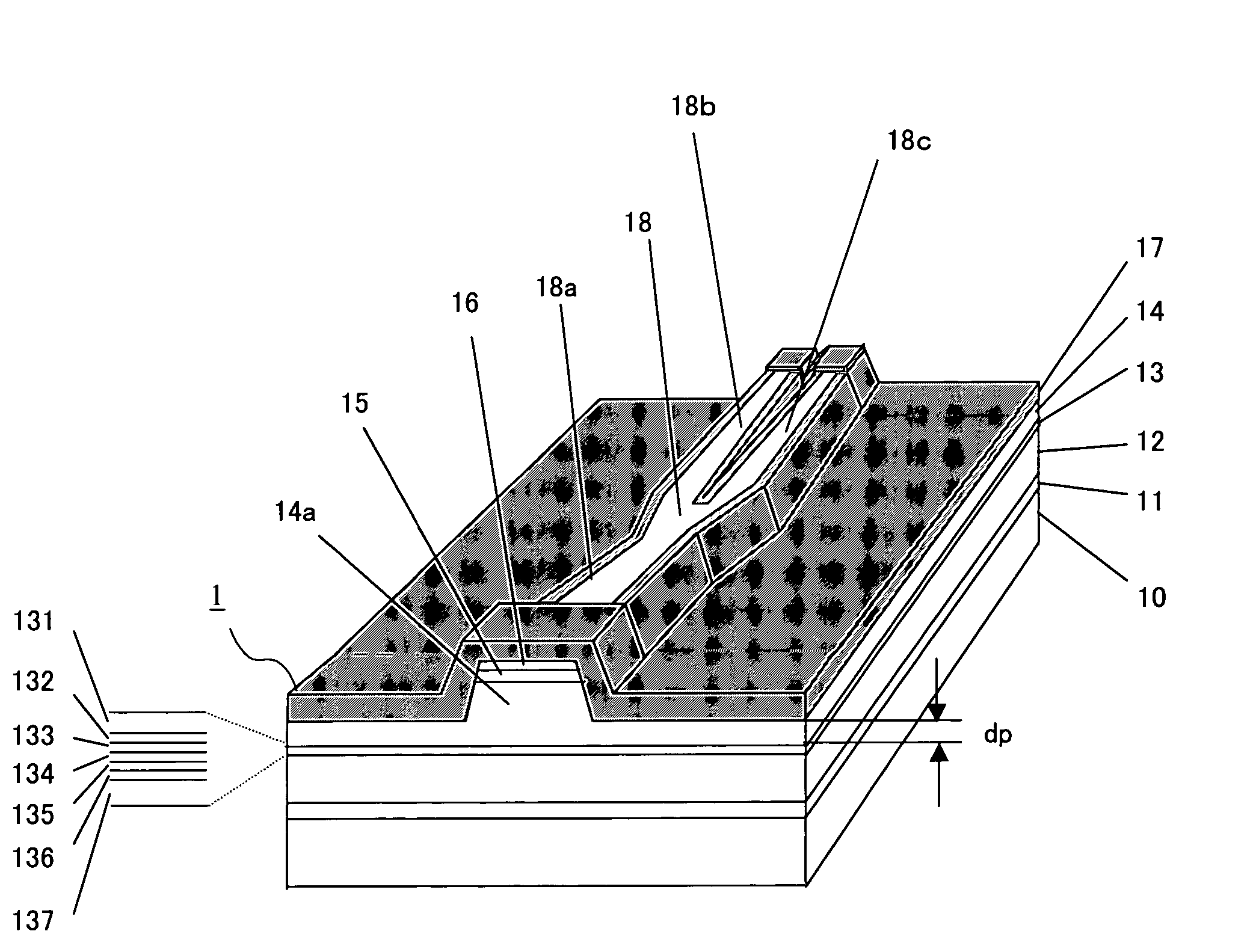
[0040]FIG. 1 shows a structure of a semiconductor laser device of Embodiment 1. A semiconductor laser device 1 of Embodiment 1 is formed on an n-type GaAs substrate 10 whose principal plane is inclined from the (100) plane by 10° in the [011] direction. An n-type GaAs buffer layer 11, an n-type (AlGa)InP first cladding layer 12, an active layer 13, a p-type (AlGa)InP second cladding layer 14, a p-type GaInP protective layer 15 and a p-type GaAs contact layer 16 are layered on the n-type GaAs substrate 10 in this order from the substrate side. The semiconductor laser device 1 has a double hetero structure including the active layer 13 and the two cladding layers sandwiching the active layer 13 therebetween.

[0041] The p-type (AlGa)InP second cladding layer 14 includes a ridge 14a having a forward mesa shape above the active layer 13. An n-type AlInP current blocking layer 17 is formed on the side surface of the ridge 14a so as to cover the ridge 14a. By a waveguide branching portion ...

embodiment 2

[0078] An example of a method for manufacturing a semiconductor laser device will now be described. FIGS. 8A to 8D are cross-sectional views each showing a step in the method for manufacturing a semiconductor laser device as described in Embodiment 1. First, the n-type GaAs buffer layer 11 (0.5 μm), the n-type (AlGa)InP first cladding layer 12 (1.2 μm), the active layer 13, the p-type (AlGa)InP second cladding layer 14, the p-type GaInP protective layer 15 (50 nm) and the p-type GaAs contact layer 16 (0.2 μm) are formed on then-type GaAs substrate 10 whose principal plane is inclined from the (100) plane by 100° in the [011 ] direction (deposition step: FIG. 8A). Each numerical value in parenthesis denotes the thickness of a layer. The composition ratio of each layer is not shown herein. The active layer 13 may be, for example, an active layer similar to the strained quantum well active layer of Embodiment 1. Note that composition ratios as those of Embodiment 1 may be used, for exa...

embodiment 3

[0084]FIG. 9 is a schematic diagram showing an optical pickup device of Embodiment 3. The optical pickup device of Embodiment 3 includes the semiconductor laser device 1 being the light source, a light receiving section 33, a diffraction grating 40, a lens element 41 and a lens element 42.

[0085] The semiconductor laser device 1 has a configuration as described above in Embodiment 1, and is provided on a substrate 30 together with the light receiving section 33 including a photodiode. The semiconductor laser device 1 is placed on a base 31 so as to suppress the influence of radiated laser light 35 being reflected off the substrate 30. A reflective surface 32 is formed between the semiconductor laser device 1 and the light receiving section 33 for bending the optical path of the laser light 35 radiated from the semiconductor laser device 1. The reflective surface 32 is formed between the position where the semiconductor laser device 1 is placed and the position where the light receiv...


PUM


Abstract

The present invention provides a semiconductor laser device having a high reliability and desirable temperature characteristics while being a high-power device. An active layer, and two cladding layers sandwiching the active layer therebetween are formed on a substrate. One of the cladding layers forms a mesa-shaped ridge, and the ridge includes a waveguide region diverging into at least two branches. With this configuration, the density of carriers injected into the rear facet portion of the active layer is decreased, whereby it is possible to improve the temperature characteristics of the semiconductor laser. While the device includes a region across which the ridge bottom width varies continuously, the ridge bottom width is constant near the facet.

Description

BACKGROUND OF THE INVENTION [0001] 1. Field of the Invention [0002] The present invention relates to a semiconductor laser device and a method for manufacturing the same and, more particularly, to a semiconductor laser device suitable for use in an optical pickup device and a method for manufacturing the same. The present invention relates also to an optical pickup device using such a semiconductor laser device. [0003] 2. Description of the Background Art [0004] Semiconductor laser devices are widely used in various fields of application. Particularly, AlGaInP semiconductor laser devices, which are capable of outputting laser light having a wavelength in a 650 nm band, are widely used as light sources of optical disk systems. In recent years, GaN semiconductor laser devices have been proposed in the art, which are capable of outputting laser light having a wavelength in a 405 nm band, and further performance improvements are expected in optical disk systems. [0005] A known type of s...

Claims


Application Information

Patent Timeline
IPC IPC(8): H01S5/00
CPCH01S5/22
Inventor TAKAYAMA, TORU
Owner PANASONIC CORP
Why Eureka
Try Eureka