OLED anode modification layer

a technology of anode modification and anode layer, which is applied in the direction of thermoelectric devices, discharge tube luminescnet screens, natural mineral layered products, etc., can solve the problems of high drive voltage, low operational life, and inability to effectively use anode as a prepared or clean on

Inactive Publication Date: 2006-10-26
EASTMAN KODAK CO
View PDF9 Cites 38 Cited by
  • Summary
  • Abstract
  • Description
  • Claims
  • Application Information

AI Technical Summary

Problems solved by technology

However, the as-prepared or clean ITO cannot be used as an effective anode because of its relatively low work function.
The low work function anode will form a high barrier for holes to inject from the anode into the adjacent organic EL unit, resulting in high drive voltage and low operational lifetime.
However, oxygen treatments are difficult to provide precise oxygen content on anode surface because many factors, such as different initial anode surface conditions, deviations on physical position during oxygen treatment, and deviations on plasma intensity, can influence the process.
As a result, the anode surface modification cannot be reproducible causing different work function on different anode surface.
Moreover, the oxygen-rich anode surface is not stable.
The oxygen on the surface will diff

Method used


Image

  • OLED anode modification layer
  • OLED anode modification layer
  • OLED anode modification layer

Examples


example 3 (

Inventive)

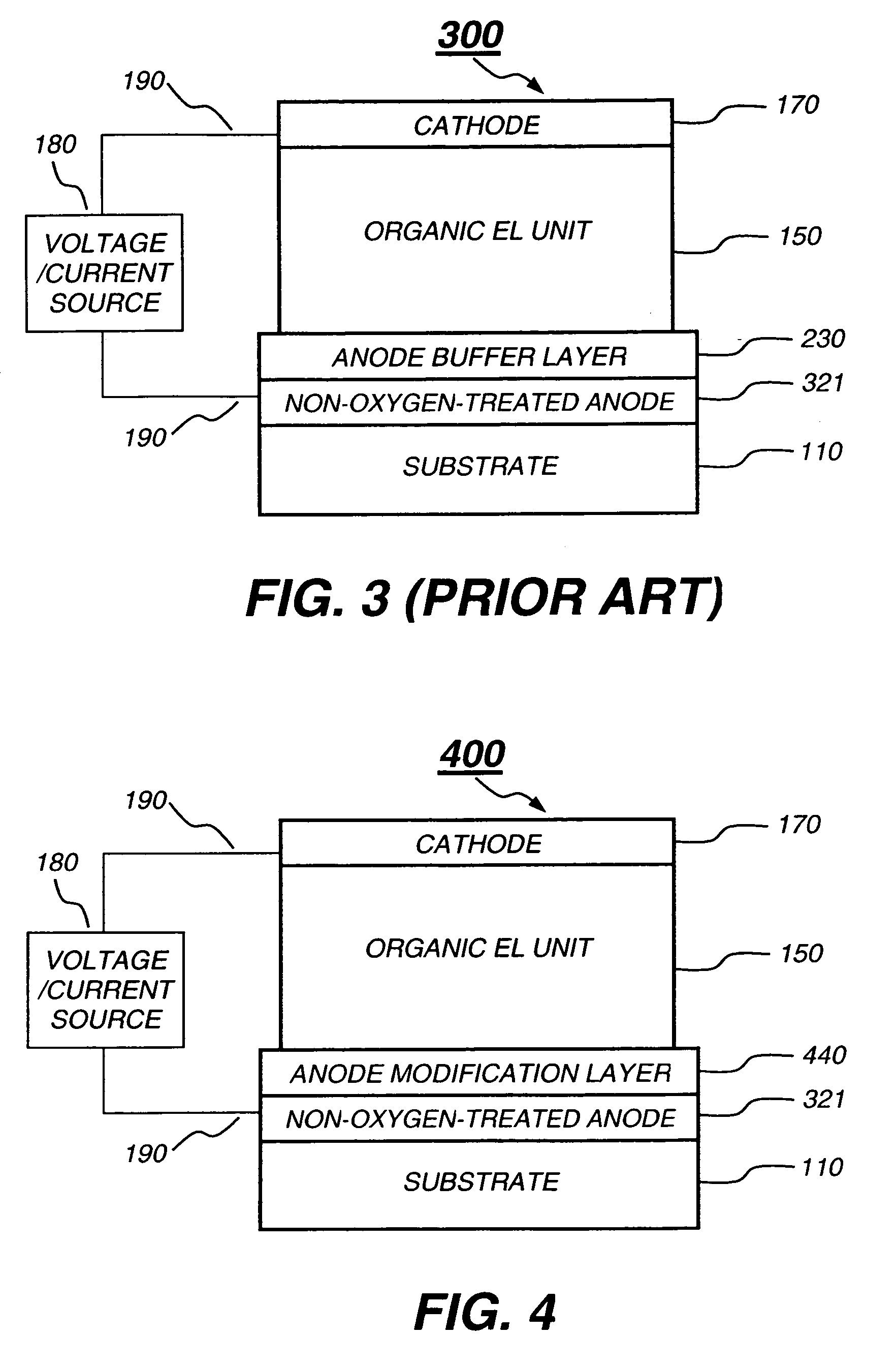
[0135] An OLED in accordance with the present invention was constructed as the same as that in Example 1, except that an anode modification layer with 0.2-nm-thick F4-TCNQ was subsequently deposited on the non-oxygen-treated ITO surface before the deposition of the organic EL unit. The reduction potential of F4-TCNQ was measured as about 0.64 V vs. SCE in the 1:1 MeCN / MePh organic solvent system.

[0136] This OLED, having an anode modification layer in direct contact with the non-oxygen-treated anode, requires a drive voltage of about 4.9 V to pass 20 mA / cm2. Under this test condition, the device has a luminance of 1933 cd / m2, and a luminous efficiency of about 9.7 cd / A. Its emission peak is at 520 nm. The operational lifetime, measured as T50(RT@80 mA / cm2), is about 320 hours (Just for a convenient comparison, it is worthwhile to know that if this device were operated at room temperature and at 20 mA / cm2, its operational lifetime would be at least 6 time longer, i.e. its T...

example 7 (

Inventive)

[0150] An OLED, having an anode modification layer in direct contact with a non-oxygen-treated anode, was constructed in accordance with the present invention. This OLED is the same as that in Example 4, except that 1) a layer of hexanitrile hexaazatriphenylene, 10 nm thick, was deposited on the non-oxygen-treated ITO surface as the anode modification layer, and 2) the thickness of the HTL (NPB layer) in the organic EL unit was reduced from 75 nm to 65 nm.

[0151] This OLED requires a drive voltage of about 6.2 V to pass 20 mA / cm2. Under this test condition, the device has a luminance of 1703 cd / m2, and a luminous efficiency of about 8.5 cd / A. Its emission peak is at 520 nm. The operational lifetime, measured as T50(RT@80 mA / cm2), is about 188 hours. Its luminance vs. operational time and its drive voltage vs. operational time, tested at room temperature and at 80 mA / cm2, are shown in FIGS. 12 and 13, respectively.

example 9 (

Inventive)

[0155] An OLED, having an anode modification layer in direct contact with a non-oxygen-treated anode, was constructed in accordance with the present invention. This OLED is the same as that in Example 7 and was used for high temperature test.

[0156] This OLED requires a drive voltage of about 6.3 V to pass 20 mA / cm2. Under this test condition, the device has a luminance of 1755 cd / m2, and a luminous efficiency of about 8.8 cd / A. Its emission peak is at 520 nm. The operational lifetime, measured as T50(85° C.@80 mA / cm2), is about 12 hours. Its luminance vs. operational time and its drive voltage vs. operational time, tested at 85° C. and at 80 mA / cm2, are shown in FIGS. 14 and 15, respectively.


PUM

PropertyMeasurementUnit
Thicknessaaaaaaaaaa
Thicknessaaaaaaaaaa
Electric potential / voltageaaaaaaaaaa

Abstract

An OLED includes an anode formed over a substrate, wherein the anode is a non-oxygen-treated anode and an anode modification layer formed in direct contact with the anode, wherein the anode modification layer includes one or more organic materials, each having an electron-accepting property and a reduction potential greater than 0.0 V vs. a Saturated Calomel Electrode, and wherein the one or more organic materials provide more than 50% by mole ratio of the anode modification layer. The OLED also includes an organic electroluminescent unit formed over the anode modification layer, wherein the organic electroluminescent unit includes at least a hole-transporting layer and a light-emitting layer, and a cathode formed over the organic electroluminescent unit.

Description

CROSS REFERENCE TO RELATED APPLICATIONS [0001] Reference is made to commonly assigned U.S. patent application Ser. No. ______ (Docket 89288) filed concurrently herewith by Liang-Sheng Liao et al., entitled “Contaminant-Scavenging Layer on OLED Anodes”, the disclosure of which is herein incorporated by reference.FIELD OF INVENTION [0002] The present invention relates to simplifying the fabrication of an organic light-emitting device (OLED). BACKGROUND OF THE INVENTION [0003] Multiple-layered organic light-emitting devices or organic electroluminescent (EL) devices, as first described by Tang in commonly assigned U.S. Pat. No. 4,356,429, are used as color pixel components in OLED displays and are also used as solid-state lighting sources. OLEDs are also useful for some other applications due to their low drive voltage, high luminance, wide viewing angle, fast signal response time, and simple fabrication process. [0004] A typical OLED includes two electrodes and one organic EL unit dis...

Claims


Application Information

Patent Timeline
IPC IPC(8): H01L51/54H05B33/12
CPCH01L51/0062H05B33/26H01L51/5206H01L51/0064H10K85/652H10K85/649H10K50/17H10K50/81H10K2101/50
Inventor LIAO, LIANG-SHENGKLUBEK, KEVIN P.SLUSAREK, WOJCIECH K.
Owner EASTMAN KODAK CO
Why Eureka
Try Eureka