[0010] It is desirable to provide a surface emitting semiconductor laser which can perform
laser oscillation in a single peak beam like a single lateral mode and a manufacturing method of a surface emitting semiconductor laser whereby such a surface emitting semiconductor laser can be easily manufactured at a high yield.
[0011] It is also desirable to provide a manufacturing method of an
electron device whereby
electron devices such as transistors and the like can be easily separated.
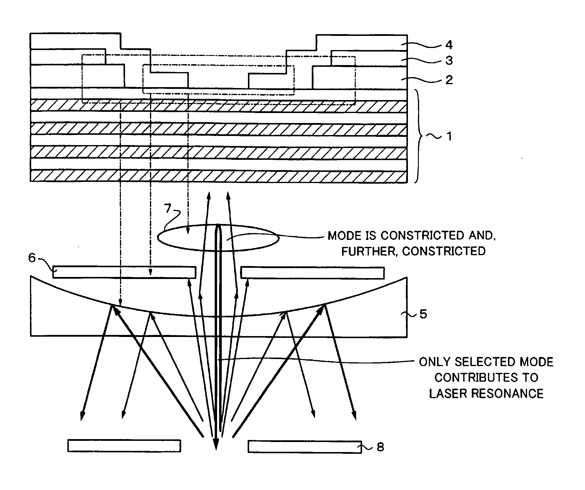
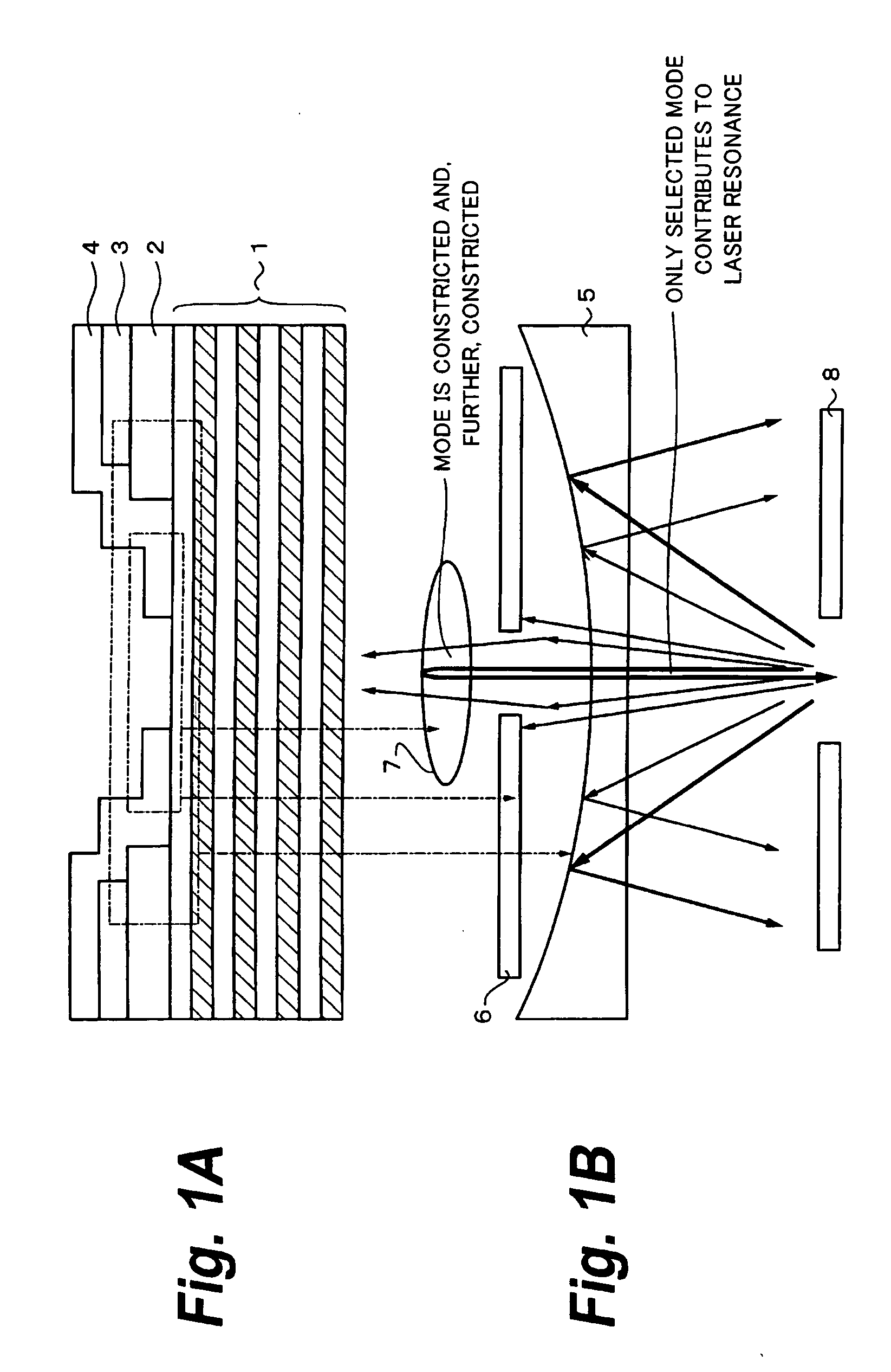
[0014] The inventors of the present invention have further examined on the basis of the above study, so that they have found a method whereby, in order to further improve the foregoing effects, by forming the
refractive index distribution like that of a concave lens to the light outgoing plane itself, the effect is given to the oscillating light mode itself, thereby suppressing the higher-order mode and realizing the single mode. It has been found that, in order to form the
refractive index distribution like that of the concave lens to the light outgoing plane, it is effective to oxidize the light outgoing plane by subject it to an oxidizing
atmosphere, particularly, a steam
atmosphere while irradiating light to the light outgoing plane.
[0015] That is, although AlGaAs is used for the light outgoing plane in, for example, GaAs VCSEL (
wavelength is equal to 850 nm), GaInNAs VCSEL (
wavelength is equal to 1300 nm), or the like, it is known that such AlGaAs fetches
oxygen of an atmosphere such as an air and naturally oxidizes it. Particularly, when a quantity of Al composition is large, such oxidization is remarkable and a mechanism for oxidization used for the current
constriction of VCSEL is the same as that of such oxidization. It has also been well-known that AlGaAs can be easily oxidized through the
moisture in the atmosphere and an oxidizing reaction progresses when a temperature is high. It is a well-known fact that prior to shipping a
semiconductor device as well as the surface emitting laser, what is called burn-in in which by setting the device into a current supplying state at a high temperature and holding it for a predetermined time, subsequent characteristics become stable is effective.
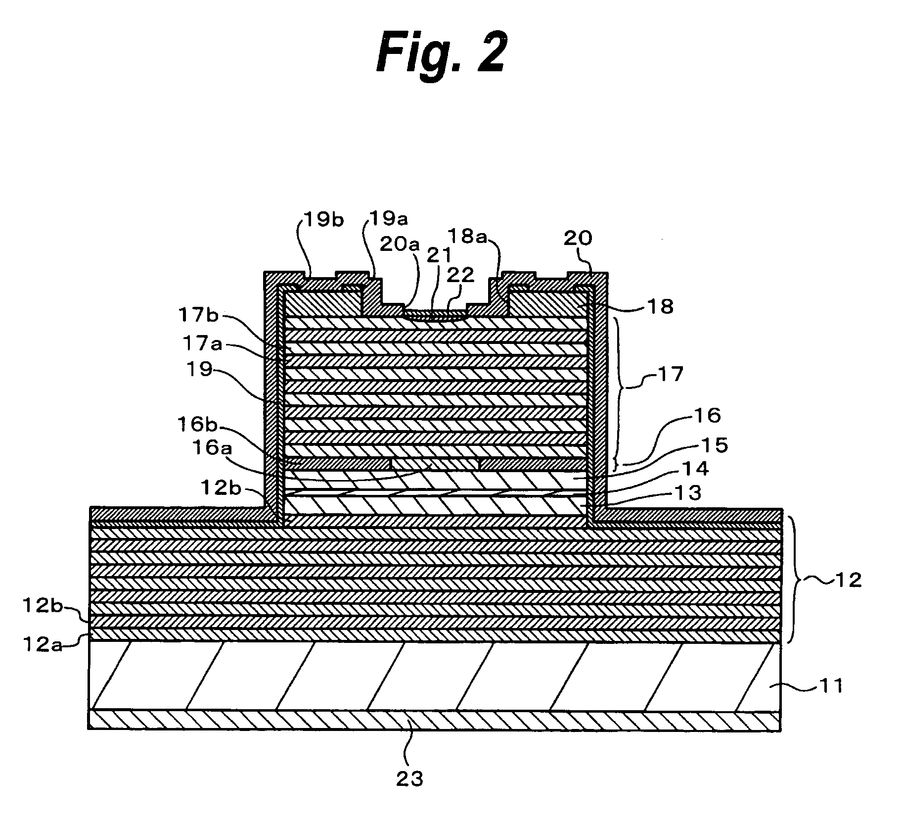
[0031] Typically, although the oxidization is executed in order to form the
oxide layer while extracting the output light having the predetermined intensity distribution from the second reflective layer, a similar effect can be obtained by oxidizing while irradiating the light having the predetermined intensity distribution from the outside. Preferably, the oxidization is executed by irradiating the light having the predetermined intensity distribution in the steam atmosphere. Preferably, the steam atmosphere of a temperature of 60° C. or more and a
humidity of 60% or more is used as a steam atmosphere. Typically, the
compound semiconductor layer containing Al is formed in the top portion of the second reflective layer and the
compound semiconductor layer containing Al is oxidized while irradiating the light having the predetermined intensity distribution, thereby forming the
oxide layer. After the oxide layer is formed, in order to suppress the progress of the subsequent oxidization and stabilize such a state, preferably, a protective film such as SiNx film formed by a CVD method or the like or
organic film formed by a
coating method or the like is formed, thereby covering the oxide layer. The oxide layer is formed, preferably, in the state of a
wafer.
[0037] According to the embodiments of the invention, by setting the refractive index distribution of the oxide layer to the refractive index distribution like that of the concave lens, the higher-order mode can be suppressed at the time of the
laser oscillation and the oscillation in the single mode can be performed. Therefore, the surface emitting semiconductor laser which can perform the
laser oscillation in the single peak beam like that of a single lateral mode can be obtained. The oxide layer having the target refractive index distribution can be formed by merely subjecting it to the oxidizing atmosphere while irradiating the light. There is no need to extremely reduce the current constriction
diameter in order to oscillate in the single lateral mode. Therefore, such a surface emitting semiconductor laser can be easily manufactured at a high yield. Further, in the electron devices, they can be easily separated by the oxide layer.

