Capacitive based sensing of molecular adsorbates on the surface of single wall nanotubes

a nanotube and capacitive technology, applied in the field of sensor, can solve the problems of slow response, unstable conductive particle/polymer interface, and difficult low-vapor-pressure materials such as explosives

Inactive Publication Date: 2006-11-09
THE UNITED STATES OF AMERICA AS REPRESENTED BY THE SECRETARY OF THE NAVY
View PDF11 Cites 51 Cited by
  • Summary
  • Abstract
  • Description
  • Claims
  • Application Information

AI Technical Summary

Problems solved by technology

Sorption-based sensors provide sensitive detection for vapors ranging from volatile organic compounds to semi-volatile chemical nerve agents, although low-vapor-pressure materials such as explosives are challenging because they do not produce a sufficiently high concentration of vapor.
Chemiresistors are simple to implement, but can suffer from instability of the conductive particle / polymer interface, slow response and insufficient sensitivity.
Microresonators can suffer from instability in the resonator-coating interface and are higher power devices.
Chemicapacitors are more stable but can suffer from slow response.
As with chemiresistors, this slow response is a result of the time necessary to load and then remove the analyte from the relatively thick layers of chemoselective material (˜1 μm) that are typically used.
Consequently, this lateral diffusion, driven by a concentration gradient, results in a long response time (˜minutes) and limits the sensitivity.
However, SWNT chemiresistors also exhibit several undesirable properties such as a high level of 1 / f noise, slow recovery, and a susceptibility to contact effects.

Method used


Image

  • Capacitive based sensing of molecular adsorbates on the surface of single wall nanotubes
  • Capacitive based sensing of molecular adsorbates on the surface of single wall nanotubes
  • Capacitive based sensing of molecular adsorbates on the surface of single wall nanotubes

Examples


example 1

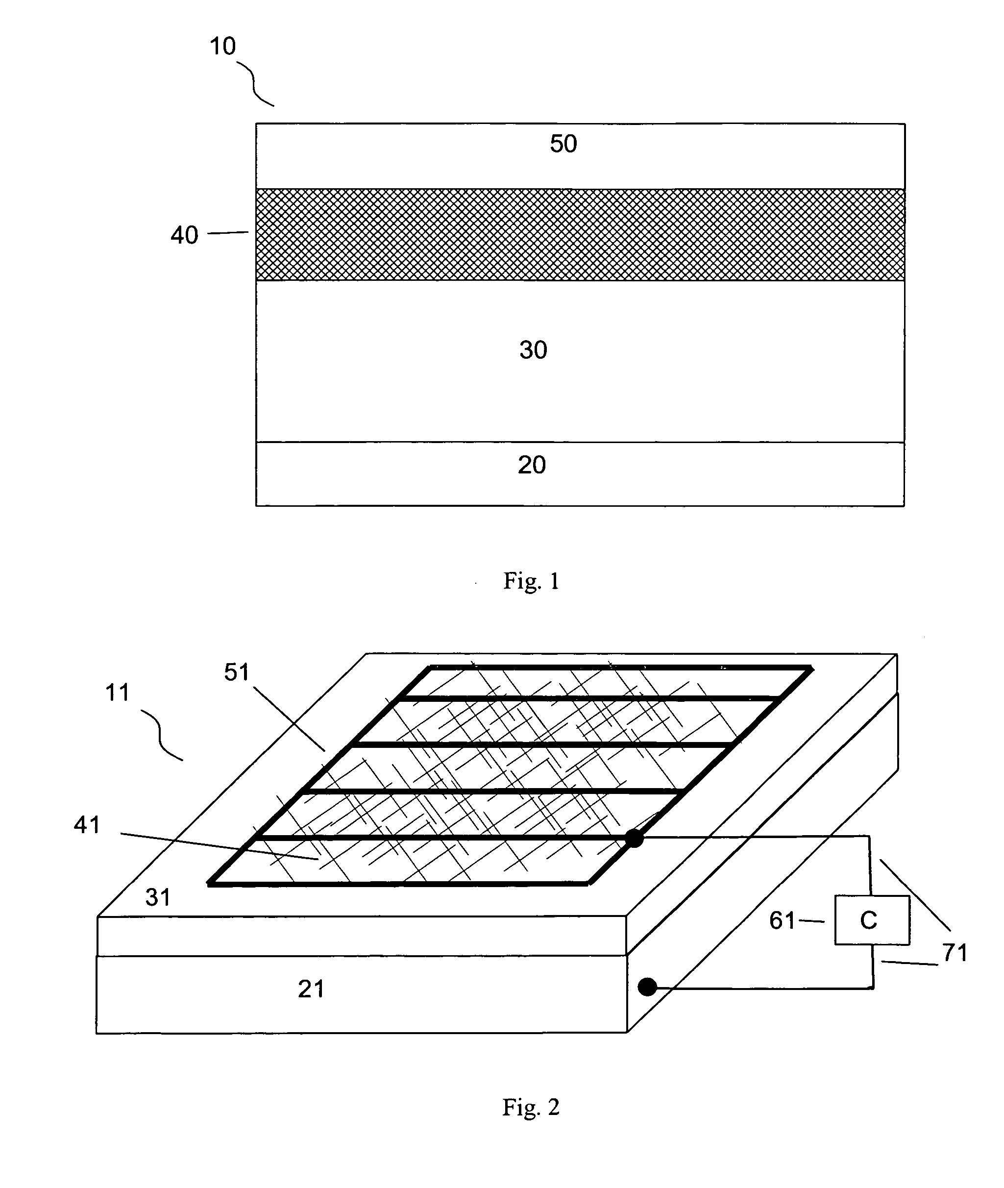
[0051] General procedure for growth of nanotube films and formation of top electrode—Select the desired substrate such as heavily doped silicon wafers with a thick thermal oxide, which may or may not be thinned to achieve a target, specific thickness. Alternatively, lightly doped silicon with patterned heavily doped areas may be used to isolate devices from one another. Alternatively, very thin, free-standing, supported films may be used.

[0052] Clean the substrate. While there exist many well-established methods of cleaning, treatment with a CO2 snow-jet process may have advantages. The function of this process, in addition to mechanical cleaning, is to charge the insulating surface.

[0053] Deposit a thin, sparse layer of growth catalyst on the surface. One process uses a solution of catalyst in alcohol: [0054] a. Prepare the catalyst solution. The catalyst solution used here is a mixture of 14 mg FeNO3:(H2O)9 in 80 mL isopropyl alcohol, stirred for at least 2 hours but generally n...

example 2

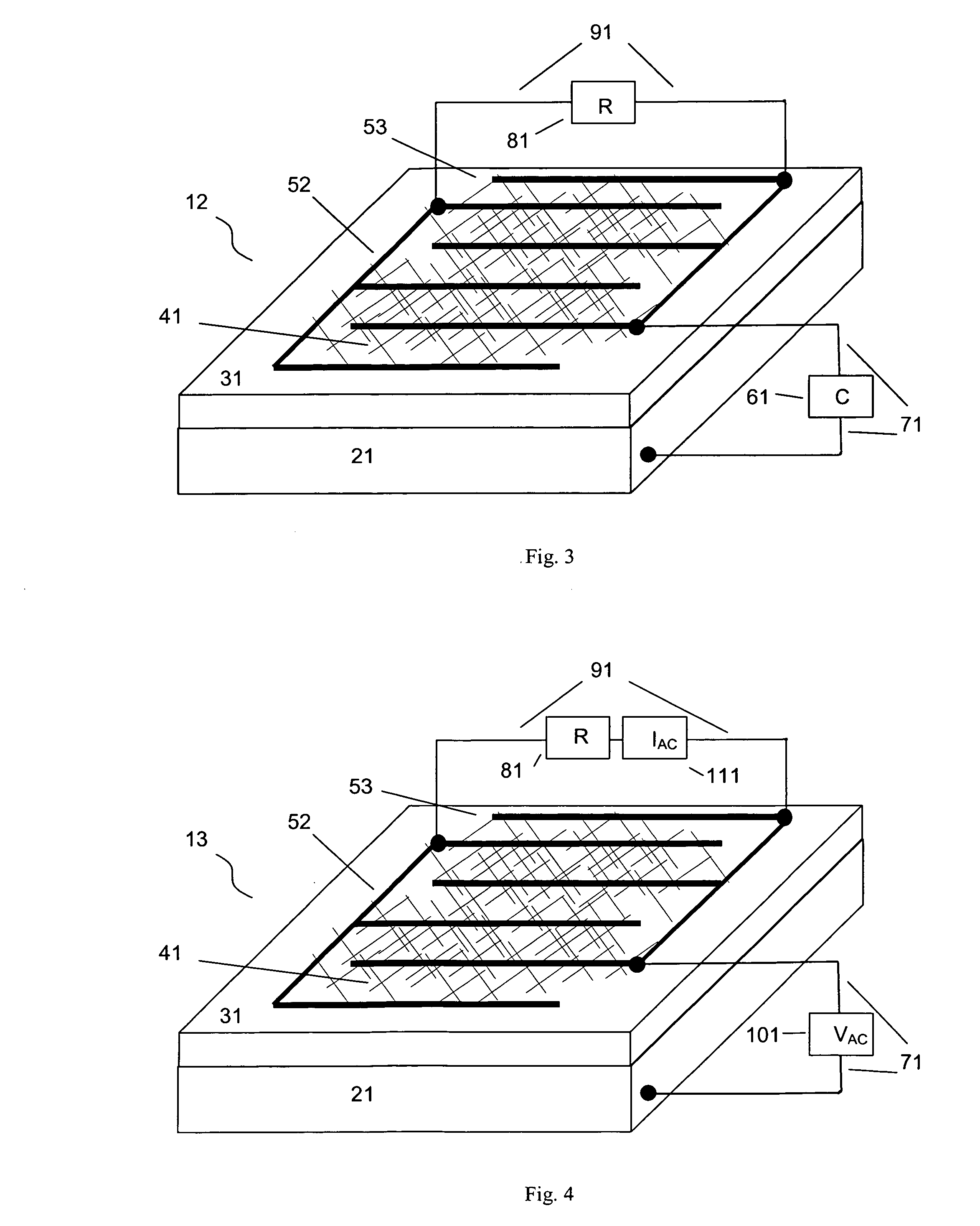
[0074] Capacitance measurement—SWNT chemicapacitors were fabricated by using chemical vapor deposition to grow a SWNT network on a 250 nm-thick thermal oxide on a highly doped silicon substrate. For each sensor a 2 mm×2 mm interdigitated array of Pd electrodes was deposited on top of the SWNT network by using photolithography and lift-off. The interdigitated electrodes provided contacts for the simultaneous measurement of both the capacitance and the resistance of the SWNT network. The region inside the array was protected by photoresist and the unprotected SWNTs were removed from the substrate by a CO2 snowjet. The photoresist was then removed exposing the SWNT network to the ambient environment. The chemical vapors were prepared by mixing saturated vapors of the analyte with dry air, and the concentrations are reported as a fraction of the equilibrium vapor pressure, P / P0.

[0075] The SWNT network formed an array of nanoscale electrodes that served as one plate of the chemicapacito...

example 3

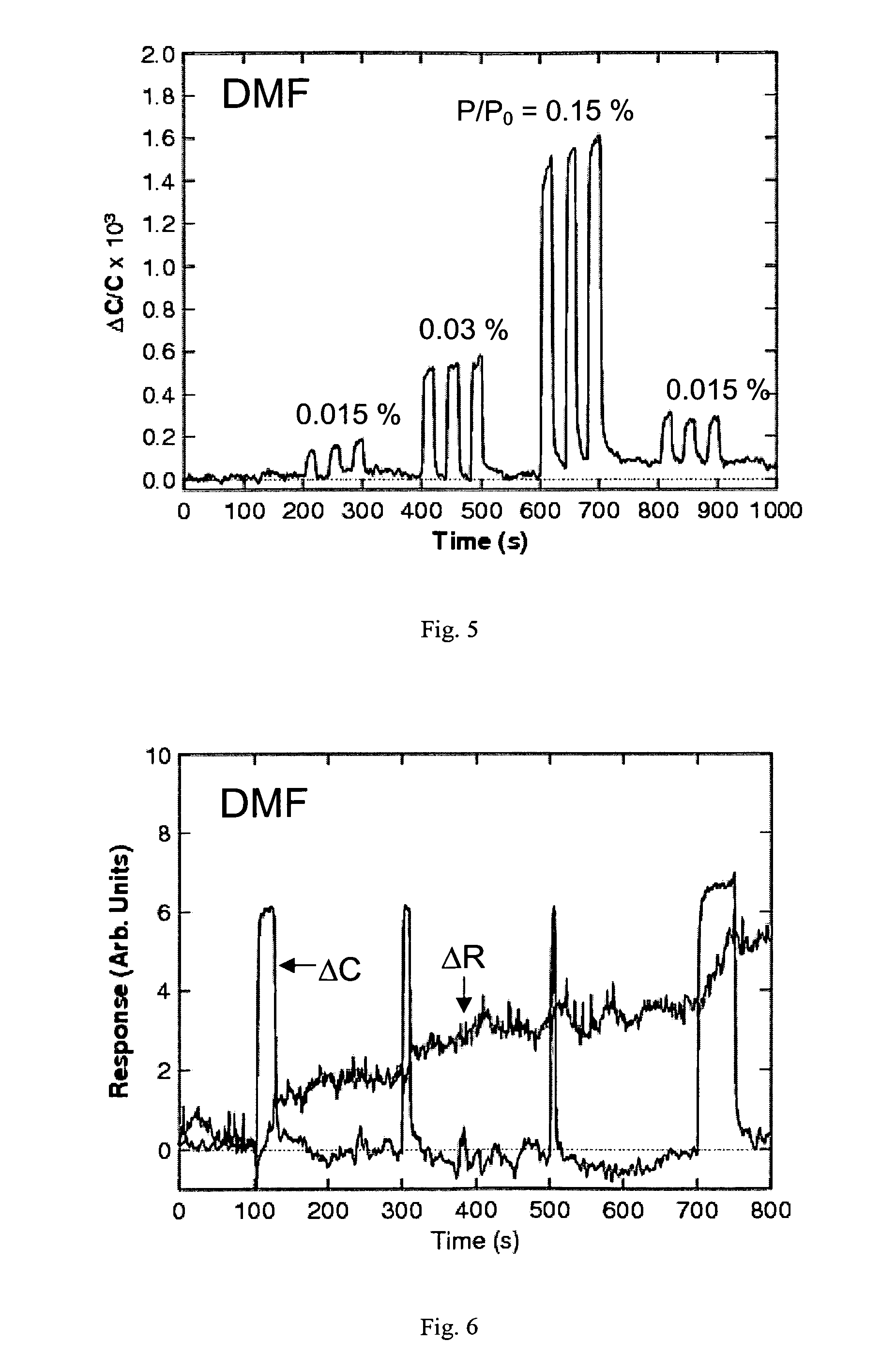
[0077] Capacitance and resistance measurement (DMF and DMMP)—FIG. 6 shows a plot of the resistance and capacitance of a SWNT network measured simultaneously in response to 25, 10, 5 and 50 s doses of DMF. The magnitude of the capacitance response is independent of the delivery time and rises and falls immediately upon the delivery and removal of the DMF. In contrast, the resistance response is much slower and behaves like a dosimeter, integrating the dose of DMF.

[0078] Different adsorption sites may have controlled the capacitance and the resistance. The DMF that affects the capacitance desorbs much faster than the DMF that affects the resistance. For the vapors tested the capacitance consistently tracks the vapor concentration in real time whereas the resistance displays a wide range of behavior. For physisorbed molecules the desorption time should be <<1 s, consistent with the capacitance measurements.

[0079] One possible explanation for the slow resistance response is that the D...


PUM

PropertyMeasurementUnit
thickaaaaaaaaaa
diameteraaaaaaaaaa
diameteraaaaaaaaaa

Abstract

A sensing device having: a bottom electrode, a dielectric on the bottom electrode, a grid of nanoelectrodes on the dielectric, and a top electrode in electrical contact with the grid. A method of chemical or biological sensing comprising: providing a grid of nanoelectrodes; exposing the grid to fluid suspected of containing a chemical or biological analyte; and measuring a change in the capacitance and conductance of the grid.

Description

[0001] The application claims the benefit of U.S. Provisional Patent Application No. 60 / 662,464 filed on Mar. 15, 2005, incorporated herein by reference.BACKGROUND OF THE INVENTION [0002] 1. Field of the Invention [0003] The invention relates generally to the field of sensors. [0004] 2. Description of the Related Art [0005] Sorption-based microsensors are currently a leading candidate for low-power, compact chemical vapor detection for defense, homeland security, and environmental monitoring applications. Such a sensor combines a nonselective transducer with a chemoselective material that serves as a vapor concentrator resulting in a highly sensitive detector that responds selectively to a particular class of chemical vapor. An array of such sensors, each coated with a different chemoselective material, produces a response fingerprint that can detect and identify an unidentified analyte. Sorption-based sensors provide sensitive detection for vapors ranging from volatile organic comp...

Claims


Application Information

Patent Timeline
Patent Type & Authority Applications(United States)
IPC IPC(8): G01N17/04
CPCB82Y15/00B82Y30/00G01N27/226Y10S977/702Y10S977/742Y10S977/92G01N27/3278
Inventor SNOW, ERIC S.PERKINS, F. KEITHHOUSER, ERICSTEPNOWSKI, STAN V.MCGILL, R. ANDREW
Owner THE UNITED STATES OF AMERICA AS REPRESENTED BY THE SECRETARY OF THE NAVY
Why Eureka
Try Eureka