Silicon nitride etching methods

Active Publication Date: 2006-11-09
IBM CORP +1
View PDF14 Cites 13 Cited by
  • Summary
  • Abstract
  • Description
  • Claims
  • Application Information

AI Technical Summary

Benefits of technology

[0008] The invention includes methods of etching silicon nitride material, and more particularly, etching nitride selective to silicon dioxide or silicide. The methods include exposing a substrate having silicon nitride thereon to a plasma including at least one fluorohydrocarbon and a non-carbon containing fluorine source such as sulfur hexafluoride (SF6). The plasma may also include oxyge

Problems solved by technology

Etching of silicon nitride material has increasingly posed challenges in the semiconductor fabrication industry.
One challenge of etching silicon nitride is maintaining selectivity.
For example, due to integration constraints (e.g., lithography overlay issues, etches of subsequent deposited layers), a silicon dioxide mask used to etch silicon nitride is typically relatively thin (e.g., 100-200 Å), which allows limited etching.
Furthermore, where silicon nitride overlays a silicide,

Method used


Image

  • Silicon nitride etching methods
  • Silicon nitride etching methods

Examples


Embodiment Construction

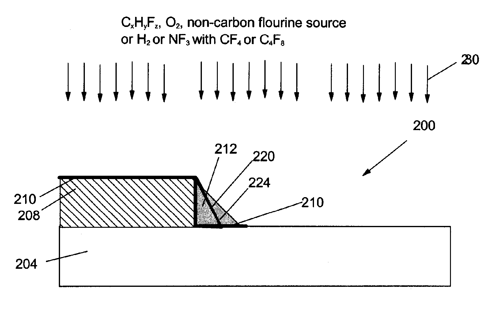
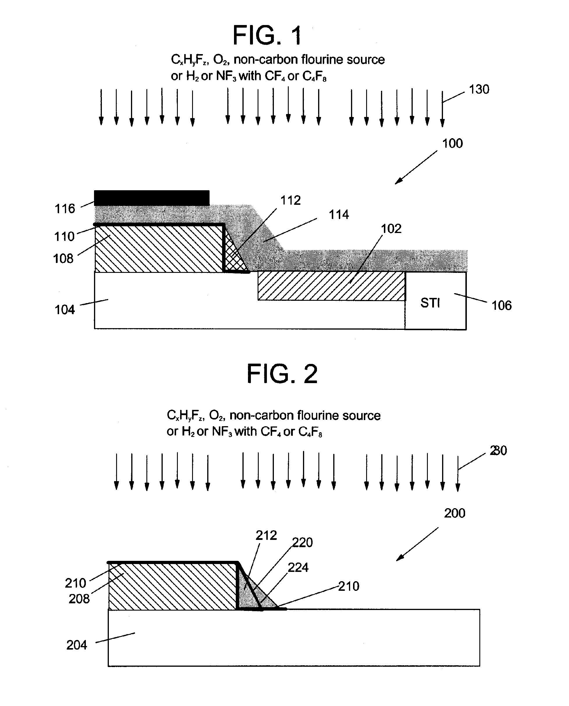
[0016] With reference to the accompanying drawings, FIGS. 1-2 show two illustrative structures for describing the methods of etching a substrate having a silicon nitride material according to the invention. It should be recognized that application of the invention is not limited to these particular structures.

[0017]FIG. 1 shows a structure 100 in the form of a silicon nitride liner scheme in which a silicide portion 102, e.g., cobalt silicide, tungsten silicide, nickel silicide, etc., is provided in a substrate 104 adjacent a shallow trench isolation (STI) 106. A gate 108 is provided on substrate 104 and includes a silicon dioxide (SiO2) protective layer 110 and a spacer 112. A liner 114 including silicon nitride material is laid over gate 108. A silicon dioxide mask 116 overlays portions of structure 100 for etching of silicon nitride liner 114. In FIG. 1, silicon nitride liner 114 is to be stripped, where exposed by mask 116. FIG. 2 shows a structure 200 in the form of a triple s...


PUM


Abstract

Methods of etching silicon nitride material, and more particularly, etching nitride selective to silicon dioxide or silicide, are disclosed. The methods include exposing a substrate having silicon nitride thereon to a plasma including at least one fluorohydrocarbon and a non-carbon containing fluorine source such as sulfur hexafluoride (SF6). The plasma may also include oxygen (O2) and the fluorohydrocarbons may include at least one of: trifluoromethane (CHF3), difluoromethane (CH2F2), and methyl fluoride (CH3F). In an alternative embodiment, the plasma includes one of hydrogen (H2) and nitrogen trifluoride (NF3) and one of tetrafluoromethane (CF4) and octafluorocyclobutane (C4F8). The methods are preferably carried out using a low bias voltage, e.g. <100 V.

Description

BACKGROUND OF THE INVENTION [0001] 1. Technical Field [0002] The present invention relates generally to methods of etching, and more particularly, to methods of etching silicon nitride material. [0003] 2. Related Art [0004] Etching of silicon nitride material has increasingly posed challenges in the semiconductor fabrication industry. One challenge of etching silicon nitride is maintaining selectivity. For example, due to integration constraints (e.g., lithography overlay issues, etches of subsequent deposited layers), a silicon dioxide mask used to etch silicon nitride is typically relatively thin (e.g., 100-200 Å), which allows limited etching. In other cases, where silicon nitride overlays a silicon dioxide, e.g., as part of a stressed nitride liner, the silicon nitride layer thickness needs to be increased to provide the required stress level to meet the device design requirements. Both these situations require a silicon nitride etch that is highly selective to the silicon dioxi...

Claims


Application Information

Patent Timeline
IPC IPC(8): H01L21/461H01L21/302
CPCH01L21/3185H01L21/31116
Inventor PANDA, SIDDHARTHAWISE, RICHARDMURTHY, SRIKANTESWARA DAKSHINASUBRAMANIAN, KAMATCHI
Owner IBM CORP
Why Eureka
Try Eureka