Light emitting element, light emitting device and manufacturing method of light emitting element

a technology of light emitting elements and manufacturing methods, which is applied in the direction of discharge tubes/lamp details, discharge tubes luminescnet screens, electric discharge lamps, etc., can solve the problems of improvement in luminous efficiency and still many problems, and achieve high luminous efficiency, high luminous quantum yield, and high luminous efficiency

Inactive Publication Date: 2006-11-23
SEMICON ENERGY LAB CO LTD
View PDF1 Cites 9 Cited by
  • Summary
  • Abstract
  • Description
  • Claims
  • Application Information

AI Technical Summary

Benefits of technology

[0038] The light emitting element of the present invention has a light emitting region of a multiple quantum well structure, and therefore, luminous efficiency thereof is high. Moreover, since the light emitting element of the present invention includes plural materials with a high luminous quantum yield, a light emitting element which emits light of a desired color, for example, white light, and which has a high luminous efficiency can be obtained.
[0039] Since the light emitting device of the present invention has a light emitting element with a high luminous efficiency, power consumption is low.
[0040] In the method for manufacturing a light emitting element according to the present invention, a light emitting region with a multiple quantum well structure containing plural materials with a high luminous quantum yield can be easily formed; thereby throughput thereof can be improved.

Problems solved by technology

However, there are still many issues.
Improvement in luminous efficiency is one of the issues.

Method used


Image

  • Light emitting element, light emitting device and manufacturing method of light emitting element
  • Light emitting element, light emitting device and manufacturing method of light emitting element
  • Light emitting element, light emitting device and manufacturing method of light emitting element

Examples


embodiment mode 1

[0059] In this embodiment mode, a light emitting element of the present invention, particularly, a light emitting region thereof is described.

[0060] The light emitting region of the light emitting element according to the present invention has a multiple quantum well structure. Specifically, the light emitting region is composed by combining a material with a high carrier transporting property which is hardly crystallized (hereinafter referred to as a host material) and a material with a high luminous quantum yield (hereinafter referred to as a guest material).

[0061] As the material with a high carrier transporting property, for example, a silicon compound such as tetraphenylsilane or tetra(3-methylphenyl)silane, an anthracene derivative such as 9,10-diphenylanthracene or 9,10-di(2-naphthyl)anthracene, a bianthryl derivative such as 10,10′-diphenyl 9,9′-dianthracene, a pyrene derivative such as 1,3,6,8-tetraphenylpyrene, a carbazole derivative such as 4,4′-di(N-carbazolyl)biphenyl...

embodiment mode 2

[0085] A vapor deposition apparatus used for implementing the present invention and a method of manufacturing a light emitting region having a multiple quantum well structure using the vapor deposition apparatus are described with reference to FIGS. 10 to 16.

[0086] In the vapor deposition apparatus used in this embodiment mode, a treatment chamber 1001 in which an object is subjected to vapor deposition and a transferring chamber 1002 are provided. The object is transferred to the treatment chamber 1001 through the transferring chamber 1002. The transferring chamber 1002 is provided with an arm 1003 for transferring the object (FIG. 10).

[0087] In the treatment chamber 1001, as shown in FIG. 11, an evaporation source 1010 for holding a first material, an evaporation source 1011a for holding a second material, an evaporation source 1011b for holding a third material, and an evaporation source 1011c for holding a fourth material are provided so as to be opposite to a holder 1014 with...

embodiment mode 3

[0118] In this embodiment mode, a light emitting element of the present invention is described.

[0119] The light emitting element of the present invention has plural layers between a pair of electrodes. The plural layers are laminated by combining layers composed of substances with a high carrier injection property and a high carrier transporting property so that a light emitting region is formed away from the electrodes, namely so that recombination of carriers is performed in a region which is away from the electrodes. The light emitting element of the present invention has a multiple quantum well structure in a light emitting region.

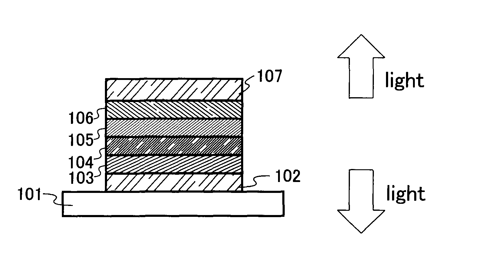
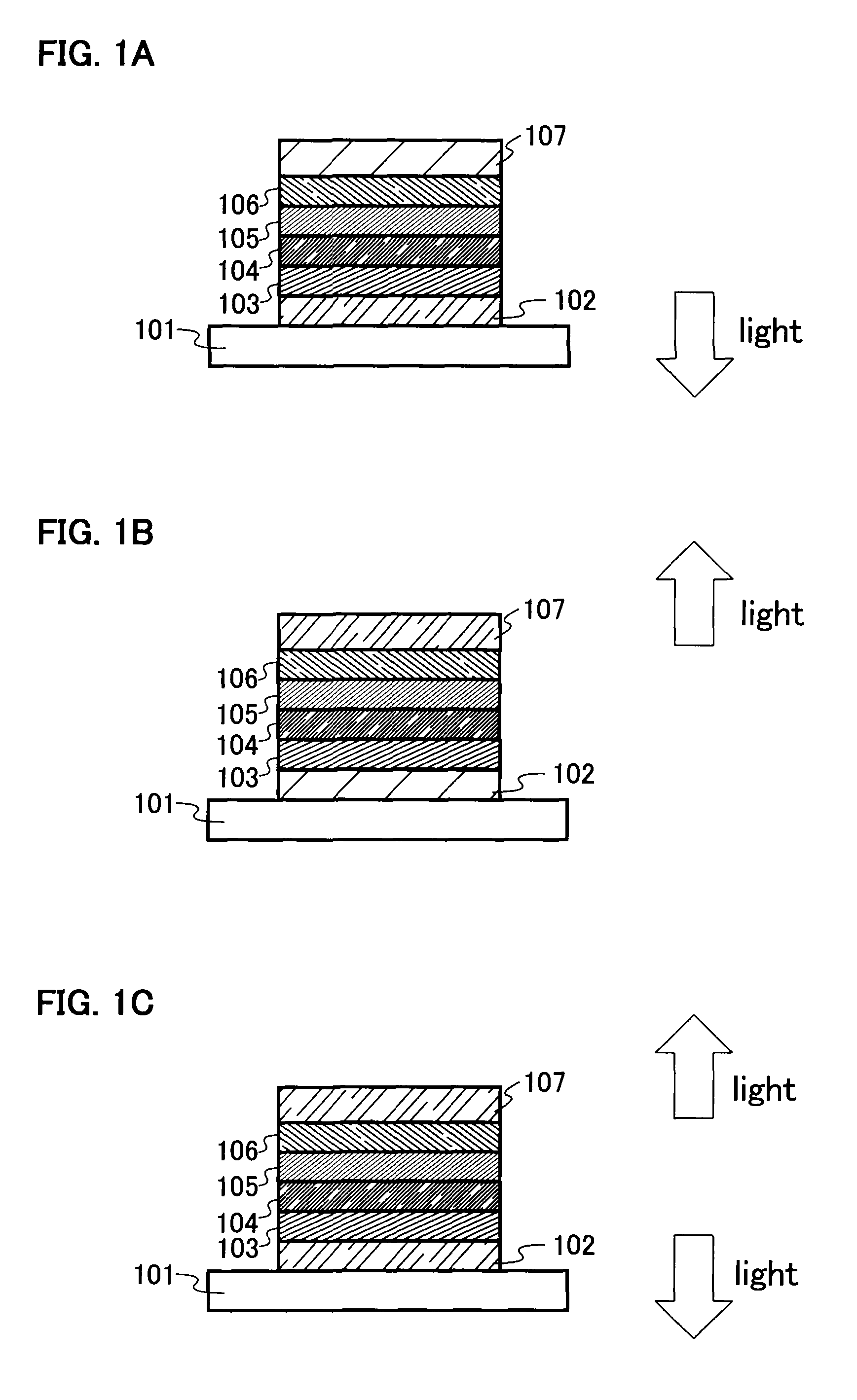
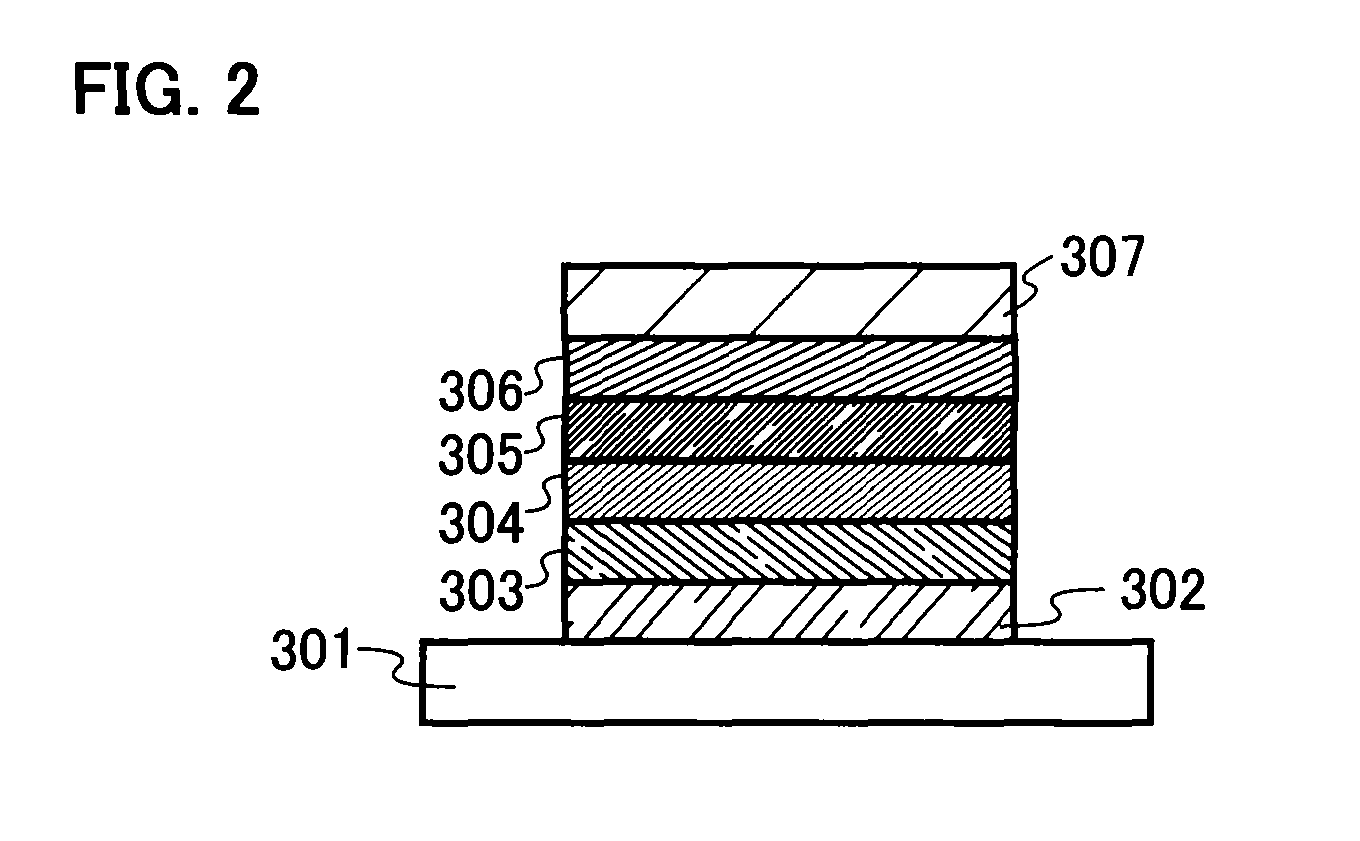
[0120] A mode of the light emitting element according to the present invention is described with reference to FIG. 1A.

[0121] In this embodiment mode, the light emitting element includes a first electrode 102, the following layers sequentially laminated over the first electrode 102: a first layer 103, a second layer 104, a third layer 105, and a four...


PUM


Abstract

It is an object of the present invention to provide a light emitting element and a light emitting device having high luminous efficiency. It is a further object of the present invention to provide a method for manufacturing the light emitting element using a simplified method compared with the conventional method. A light emitting element having a light emitting region which includes plural kinds of materials with a high luminous quantum yield, and one or plural kinds of materials with a high carrier transporting property and which has a structure where regions in which the material with a high luminous quantum efficiency is dispersed in a material with a high carrier transporting property and regions in which the concentration of the material with a high carrier transporting property is high are laminated alternately, between a pair of electrodes, is provided.

Description

BACKGROUND OF THE INVENTION [0001] 1. Field of the Invention [0002] The present invention relates to a light emitting element utilizing electroluminescence and a light emitting device provided with the light emitting element. Further, the present invention relates to a method for manufacturing the light emitting element. [0003] 2. Description of the Related Art [0004] In recent years, a light emitting element using a light emitting organic compound has been actively researched and developed. A basic structure of the light emitting element is that in which a layer containing a light emitting organic compound (light emitting layer) is sandwiched between a pair of electrodes. By applying voltage to this element, electrons and holes are separately injected from the pair of electrodes into the light emitting layer, and current flows. Then, recombination of these carriers (the electrons and holes) makes the light emitting organic compound in an excited state and emit light when the excite...

Claims


Application Information

Patent Timeline
Patent Type & Authority Applications(United States)
IPC IPC(8): H05B33/00H01L51/50
CPCH01L51/0059H01L51/0067H01L51/5036H01L51/0077H01L51/0081H01L51/0071H10K85/631H10K85/30H10K85/324H10K85/654H10K85/657H10K50/125
Inventor YAMAZAKI, SHUNPEINOMURA, RYOJIKATO, KAORU
Owner SEMICON ENERGY LAB CO LTD
Why Eureka
Try Eureka