Semiconductor optical modulator having a quantum well structure for increasing effective photocurrent generating capability

a quantum well and optical modulator technology, applied in the field of semiconductor-based optical modulators, can solve the problems of difficult extraction of electron-hole pairs and large photocurrent generation, and achieve the effects of increasing the effective photocurrent generation capability, high energy barrier, and increasing the absorption coefficient of quantum wells

Inactive Publication Date: 2006-11-30
AVAGO TECH WIRELESS IP SINGAPORE PTE
View PDF12 Cites 4 Cited by
  • Summary
  • Abstract
  • Description
  • Claims
  • Application Information

AI Technical Summary

Benefits of technology

[0007] The semiconductor optical modulator having a quantum well structure for increasing effective photocurrent generating capability substantially aligns the peaks of the wave functions of the electrons in the conduction band and the holes in the valence bands, respectively, in the quantum well. In one embodiment, the quantum well structure is formed with a quantum well layer that has a graded bandgap energy profile. In another embodiment, the quantum well structure is formed with an additional layer of material having a graded composition located adjacent the quantum well layer. The alignment of the electron and hole wave functions increases the absorption coefficient of the quantum well. The quantum well structure provides a high energy barrier at the interface of the quantum well and the barrier layer, while allowing efficient extraction of the photogenerated carriers to provide a large photocurrent.

Problems solved by technology

However, a high energy barrier at the junction of the quantum well layer and the barrier layer also makes it difficult to extract the electron-hole pairs and generate a large photocurrent.

Method used


Image

  • Semiconductor optical modulator having a quantum well structure for increasing effective photocurrent generating capability
  • Semiconductor optical modulator having a quantum well structure for increasing effective photocurrent generating capability
  • Semiconductor optical modulator having a quantum well structure for increasing effective photocurrent generating capability

Examples


Embodiment Construction

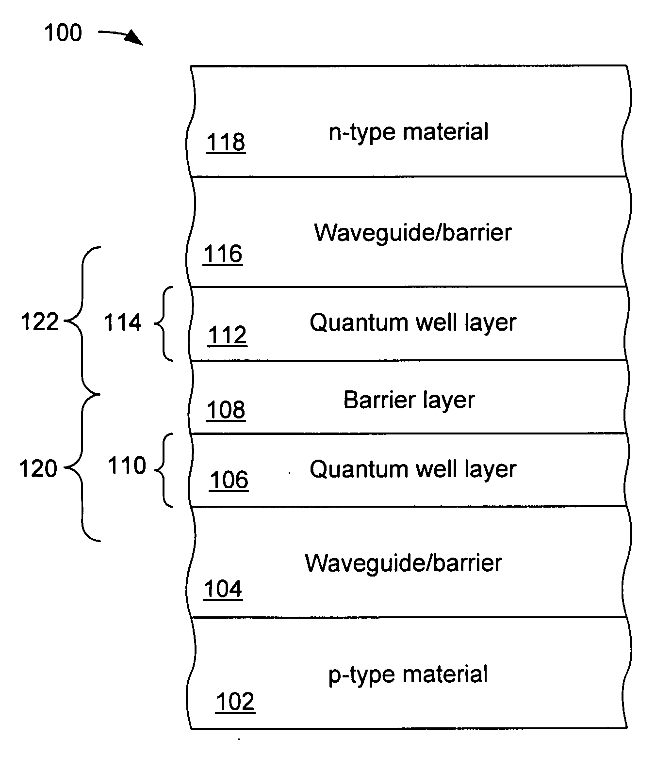
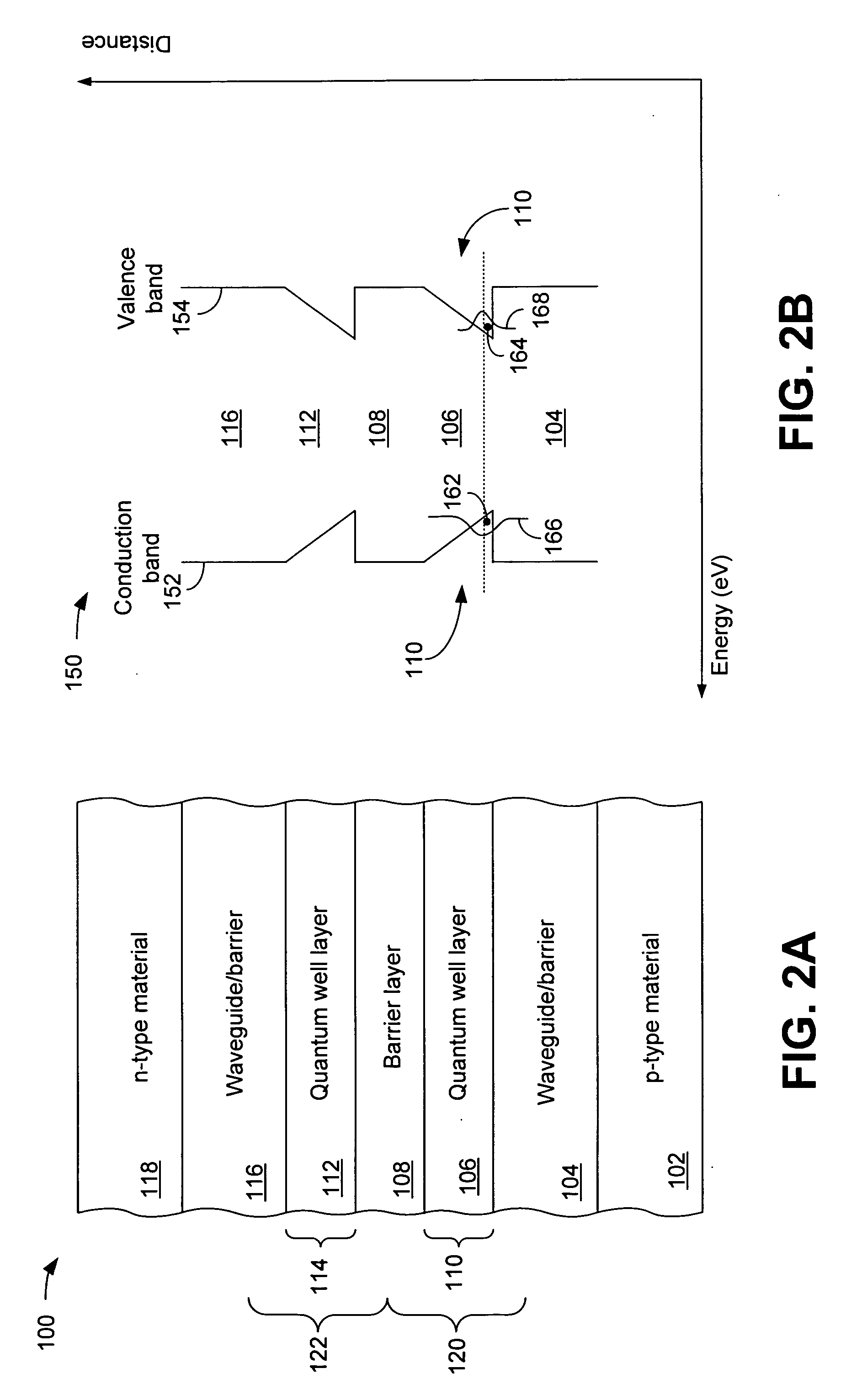
[0022] The semiconductor optical modulator having a quantum well structure for increasing photocurrent generating capability will be described below as being implemented in an indium phosphide (InP) material system, and specifically in an optical modulator fabricated using indium gallium arsenide phosphide (InGaAsP) on an InP substrate. However, the semiconductor optical modulator having a quantum well structure for increasing photocurrent generating capability can be implemented in devices fabricated using other materials, such as aluminum gallium indium arsenide (AlGaInAs).

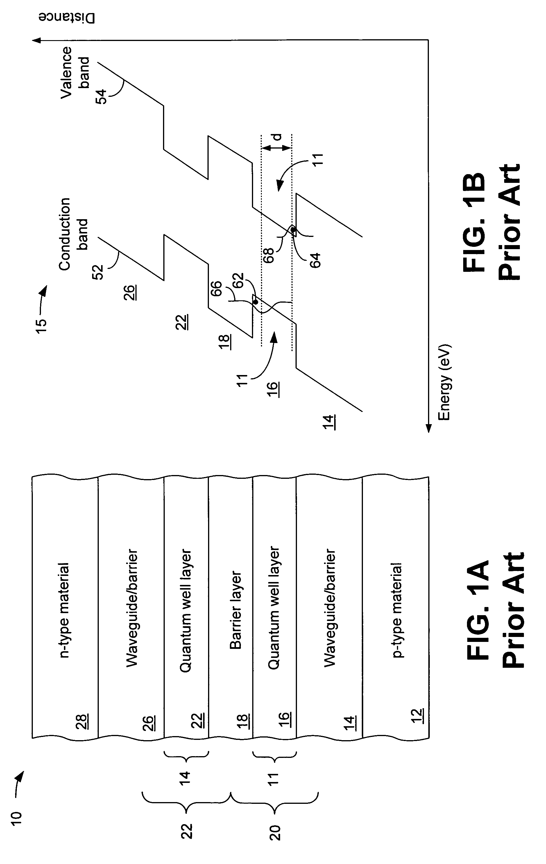
[0023]FIG. 1A is a schematic diagram illustrating a portion of a conventional semiconductor optical modulator 10. The optical modulator 10 includes a p-type material layer 12 over which a waveguide layer 14 is formed. A quantum well layer 16 is formed over the waveguide layer 14. A barrier layer 18 is formed over the quantum well layer 16. Another quantum well layer 22 is formed over the barrier layer 18 and an...


PUM

PropertyMeasurementUnit
thicknessaaaaaaaaaa
wavelengthaaaaaaaaaa

Abstract

An optical modulator comprises a first waveguide layer and a barrier layer, and a quantum well layer sandwiched between the first waveguide layer and the barrier layer, where the quantum well layer has a graded composition that varies the bandgap energy of the quantum well layer between a minimum bandgap energy and the bandgap energy of at least one of the first waveguide layer and the barrier layer.

Description

BACKGROUND OF THE INVENTION [0001] Semiconductor-based optical modulators have been developed using many different technologies and are used for modulating light for optical communications. One such semiconductor-based optical modulator is referred to as an electro-absorption modulator. In one example, a semiconductor electro-absorption optical modulator is used to modulate light in the 1550 nanometer (nm) wavelength for use in a long range fiber-optic communication system. A typical semiconductor electro-absorption optical modulator is fabricated using wafer processing technology. The optical modulator is typically reverse biased by an external electrical circuit so that when an input light source is coupled into the optical modulator, the input light is converted by one or more quantum wells in the optical modulator into a photocurrent. The wavelength of light at which the quantum wells in the optical modulator absorb photons and convert the photons to a photocurrent is dependent ...

Claims


Application Information

Patent Timeline
Patent Type & Authority Applications(United States)
IPC IPC(8): G02F1/035
CPCB82Y20/00G02F2001/01758G02F2001/0175G02F1/01725G02F1/01758G02F1/0175H01L31/02
Inventor BOUR, DAVID P.ZHU, JINTIAN
Owner AVAGO TECH WIRELESS IP SINGAPORE PTE
Why Eureka
Try Eureka