

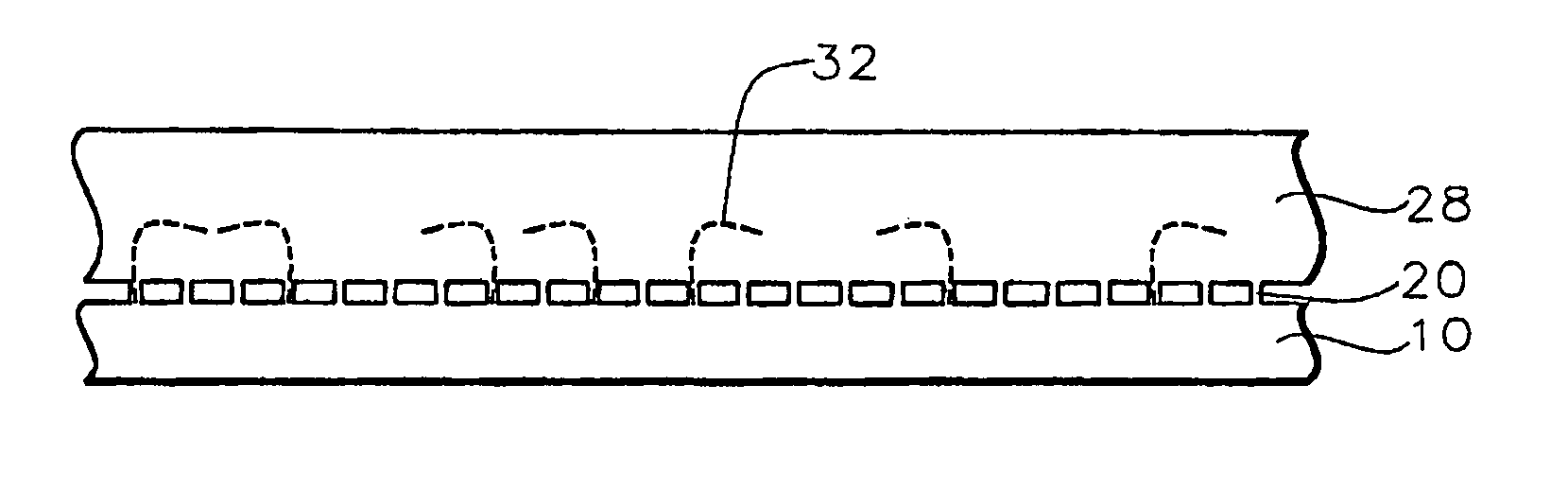
Nano-air-bridged lateral overgrowth of GaN semiconductor layer
a semiconductor layer and nano-air bridge technology, applied in the direction of single crystal growth, polycrystalline material growth, chemistry apparatus and processes, etc., can solve the problems of high dislocation density and residual strain inside the layers, poor electrical and optical properties of devices, and the rise of heteroepitaxial growth, so as to reduce the effect of eliminating contamination arising from the use of a mask (silicon dioxide or silicon nitride) and reducing dislocation density and stress
- Summary
- Abstract
- Description
- Claims
- Application Information
AI Technical Summary
Benefits of technology
Problems solved by technology
Method used
Image

Examples
example
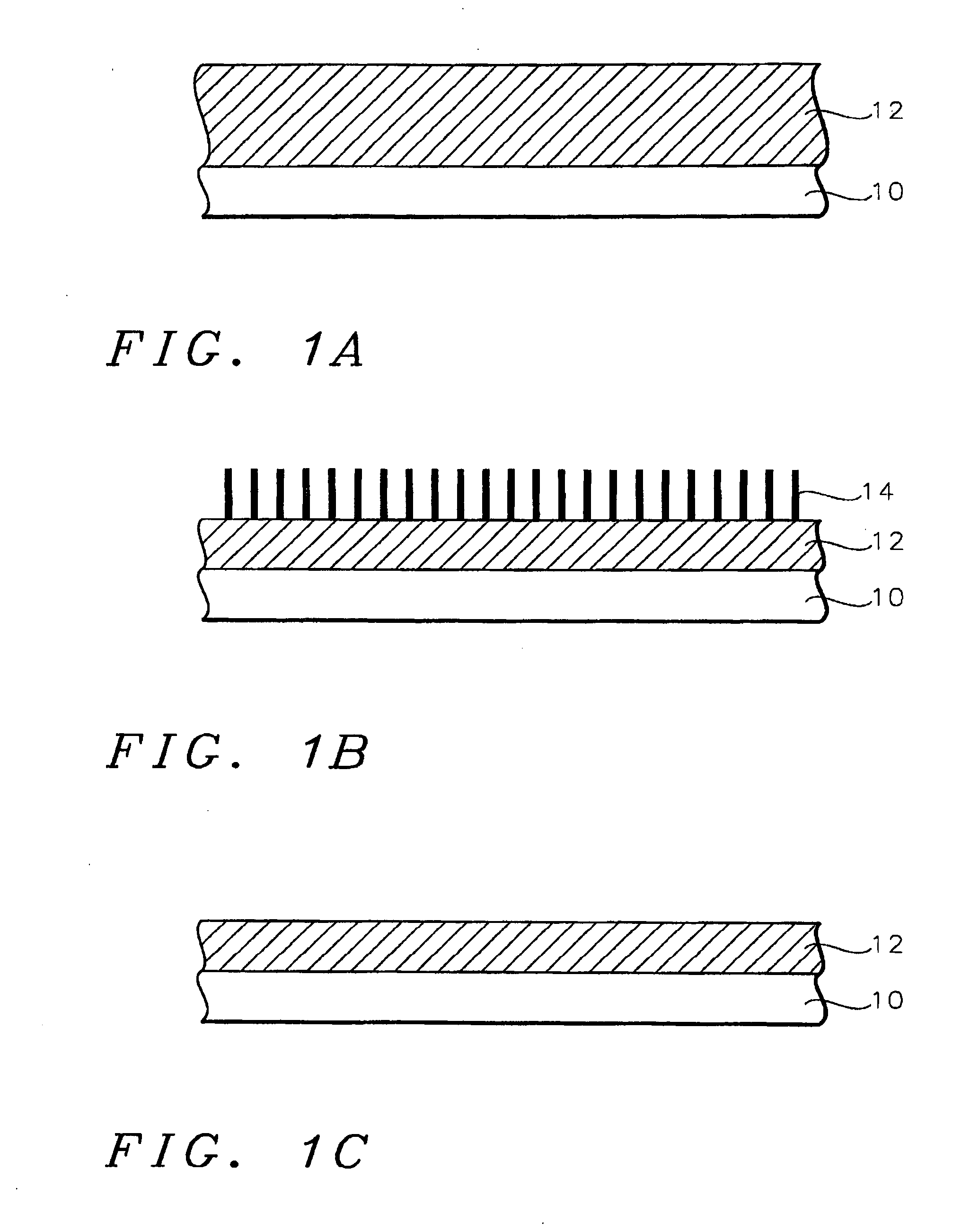
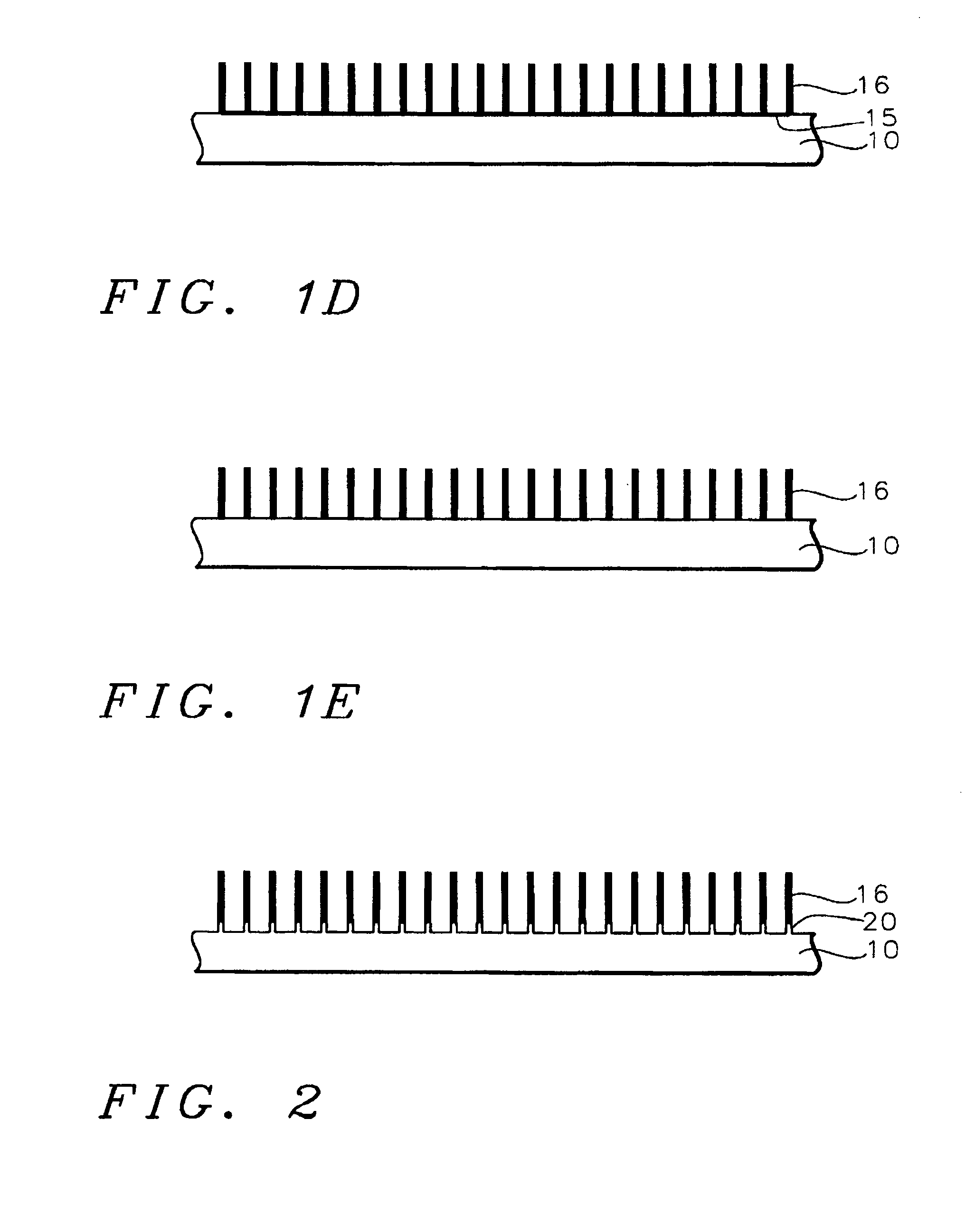
[0035] The following Example is given to show the important features of the invention and to aid in the understanding thereof. Variations may be made by one skilled in the art without departing form the spirit and scope of the invention.
[0036] In an effort to illustrate the quality of the overgrown sample, a controlled sample was also loaded into the chamber for growth under the same conditions, but without any nano-pattern on the surface. Atomic force microscope (AFM) images for the overgrown sample and control sample were obtained. The overgrown sample shows a surface that is much smoother than the control sample. Also the pit density is largely reduced in the overgrown sample. The surface root mean square (RMS) roughness is 0.25 nm and 0.39 nm for the overgrown sample and the controlled sample, respectively.
[0037] A crystallographic analysis by high-resolution x-ray diffraction rocking curves (omega scans) for both samples were obtained. X-ray diffraction is indicative of struc...
PUM
| Property | Measurement | Unit |
|---|---|---|
| thickness | aaaaa | aaaaa |
| thickness | aaaaa | aaaaa |
| RMS) roughness | aaaaa | aaaaa |
Abstract
Description
Claims
Application Information