Semiconductor device and method for manufacturing the same

Inactive Publication Date: 2006-11-30
SEMICON ENERGY LAB CO LTD
View PDF26 Cites 68 Cited by
  • Summary
  • Abstract
  • Description
  • Claims
  • Application Information

AI Technical Summary

Benefits of technology

[0051] The invention provides a semiconductor device in which a microstructure resistant to external force or stress, and a semiconductor element superior in device characteristics are formed over one substrate by using polycrystalline silicon crystallized using a metal such as nickel (Ni) for

Problems solved by technology

Further, how to seal the micr

Method used


Image

  • Semiconductor device and method for manufacturing the same
  • Semiconductor device and method for manufacturing the same
  • Semiconductor device and method for manufacturing the same

Examples


embodiment mode 1

[0070] In this embodiment mode, a configuration example of a semiconductor device according to the invention and a method for manufacturing the semiconductor device will be described with reference to drawings.

[0071] A semiconductor device of the invention is in the field of micromachines, and the size is in units of micrometer to millimeter. Further, in the case of manufacturing the semiconductor device as a component incorporated in a mechanical apparatus, a semiconductor device may be in units of meter so that it can be handled easily at the time of assembly.

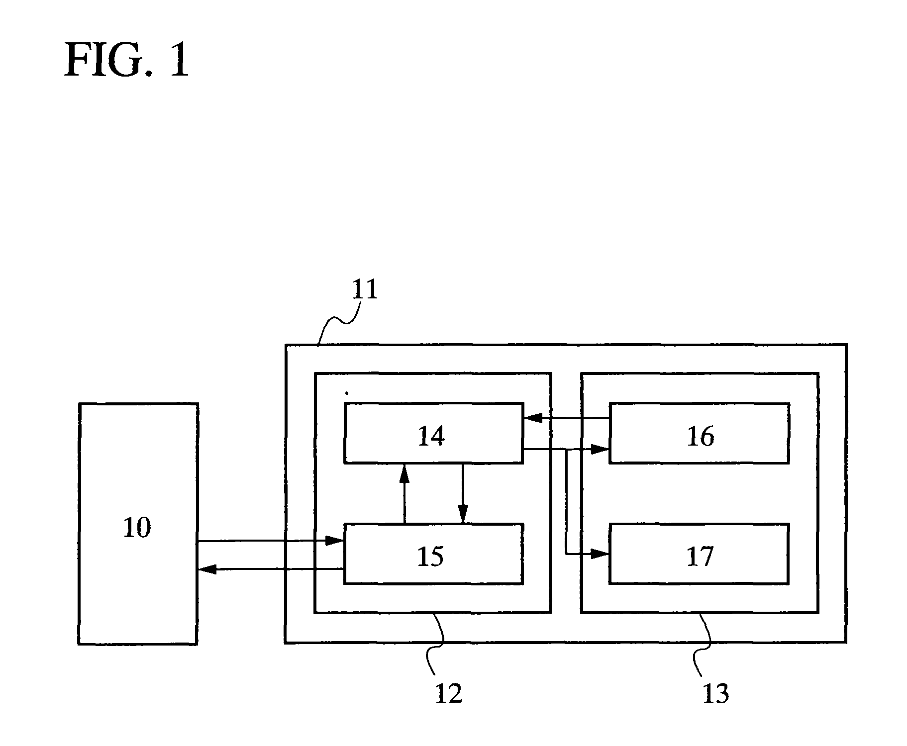
[0072]FIG. 1 shows a schematic view of a semiconductor device of the present invention.

[0073] A semiconductor device 11 of the invention has an electric circuit portion 12 including a semiconductor element and a structure portion 13 formed from a microstructure. The electric circuit portion 12 has a control circuit 14 for controlling the microstructure, an interface 15 for communicating with an external control device 10, ...

embodiment mode 2

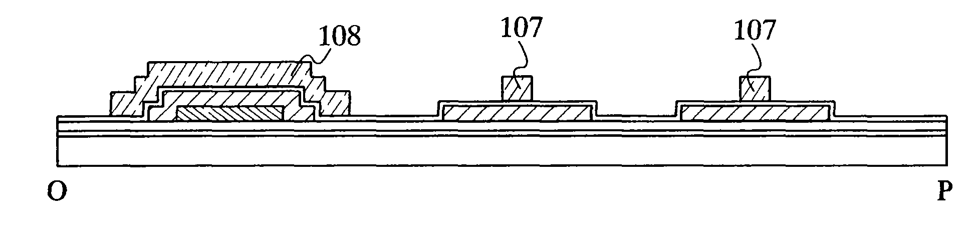
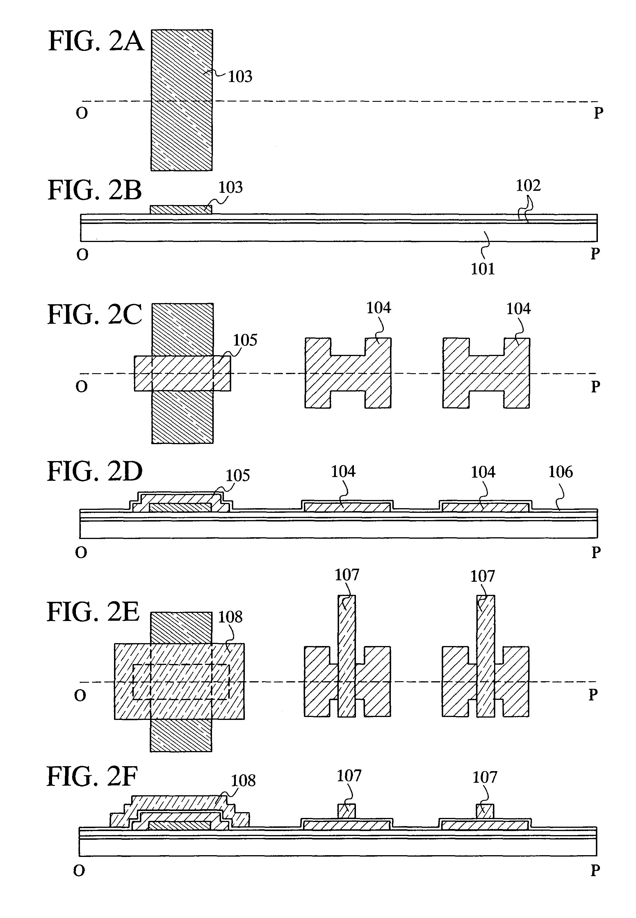
[0153] Next, a method for manufacturing a microstructure and a semiconductor element on one substrate in order to manufacture a semiconductor device of the invention described above, which is different from Embodiment Mode 1 will be described with reference to FIGS. 6A to 11C. Each of the drawings is a top view or a cross-sectional view taken along O-P or Q-R in the corresponding top view.

[0154] A microstructure and a semiconductor element of the invention can be manufactured on an insulating substrate.

[0155] First, a base film 202 is formed over a substrate having an insulating surface 201 (FIGS. 6A and 6B). The base film 202 can be formed from a single layer of an insulating layer such as a silicon oxide film, a silicon nitride film, or a silicon oxynitride film or a stack thereof. Here, the case of using a two-layer structure as in Embodiment Mode 1 for the base film 202 is described; however, the base film 202 may have a single layer structure of an insulating layer or a layer...

embodiment mode 3

[0216] In this embodiment mode, an example of a semiconductor device described in the above embodiment modes is shown. In a semiconductor device of the present invention, a sensor device 301 can be manufactured using a detector element which is formed from a microstructure.

[0217]FIG. 12A shows a structure of the sensor device 301 which is one mode of a semiconductor device of the invention. The sensor device 301 in this embodiment has an electric circuit portion 302 having a semiconductor element and a structure portion 303 including a microstructure.

[0218] The structure portion 303 has a detector element 304 formed from a microstructure, which detects external pressure, concentration of a substance, flow rate of gas or fluid, or the like.

[0219] The electric circuit portion 302 includes an AD converting circuit 305, a control circuit 306, an interface 307, a memory 308, and the like.

[0220] The AD converting circuit 305 converts information sent from the detector element into a d...


PUM


Abstract

A microstructure and a semiconductor element which are included in a micromachine have been generally formed in different steps. It is an object to provide a method for manufacturing a micromachine in which a microstructure and a semiconductor element are formed over one insulating substrate. A feature of the invention is a micromachine including a movable layer containing polycrystalline silicon which is thermally crystallized or crystallized by a laser using metal and a space below or above the layer. Such polycrystalline silicon has high strength and is formed on an insulating surface, so that it is used as a microstructure and used for forming a semiconductor element. Accordingly, a semiconductor device in which a microstructure and a semiconductor element are formed over one insulating substrate can be formed.

Description

BACKGROUND OF THE INVENTION [0001] 1. Field of the Invention [0002] The present invention relates to a semiconductor device having a microstructure and a semiconductor element over one substrate, and a method for manufacturing the same. [0003] 2. Description of the Related Art [0004] In recent years, research on micro machine systems called MEMS has been actively undertaken. MEMS is an abbreviation of MicroElectroMechanical System, and may be called simply a micromachine. A micromachine generally refers to micro devices in which a microstructure having a three dimensional structure which is movable and an electron circuit having a semiconductor element are integrated by semiconductor micromachining technologies. The above microstructure differs from a semiconductor element in having a three-dimensional structure and a movable portion. Further, it may have functions of switches, variable capacitors, actuators, and the like. [0005] Since a micromachine can control microstructures insi...

Claims


Application Information

Patent Timeline
IPC IPC(8): H01L21/311
CPCB81C1/00246B81C2203/0735H01L21/0237H01L21/02532H01L27/1277H01L21/02675H01L21/02691H01L27/1266H01L21/02672H01L21/268H01L21/20H01L21/324
Inventor IZUMI, KONAMIYAMAGUCHI, MAYUMI
Owner SEMICON ENERGY LAB CO LTD
Why Eureka
Try Eureka