Semiconductor circuit pattern design method for manufacturing semiconductor device or liquid crystal display device

a semiconductor device and circuit pattern technology, applied in the direction of cad circuit design, originals for photomechanical treatment, instruments, etc., can solve the problems of increasing the load on iteration, difficulty in faithfully forming a pattern, and increasing the chip area

Inactive Publication Date: 2006-11-30
KK TOSHIBA
View PDF7 Cites 42 Cited by
  • Summary
  • Abstract
  • Description
  • Claims
  • Application Information

AI Technical Summary

Problems solved by technology

However, as the pattern size decreases, it is becoming difficult to faithfully form a pattern in each process, and the final finished dimensions differ from the dimensions of the design pattern.
Serious problems also arise because the chip area increases as a result of buffer insertion, and the load on iteration increases due to timing closure by transistors designed in dimensions of worst conditions.
Presently, since the design pattern created by the designer largely differs from the mask pattern used for exposure because of the complex OPC and PPC technologies, the finished pattern shape on the wafer can hardly be predicted.
Feeding back the verification result indicates regress in the design step, which places a heavy load on the turnaround time of the design pattern creation step.
As described above, in the conventional pattern design method, it is not easy to predict the finished pattern shape on the wafer because the OPC and PPC technologies are complex.

Method used


Image

  • Semiconductor circuit pattern design method for manufacturing semiconductor device or liquid crystal display device
  • Semiconductor circuit pattern design method for manufacturing semiconductor device or liquid crystal display device
  • Semiconductor circuit pattern design method for manufacturing semiconductor device or liquid crystal display device

Examples


first embodiment

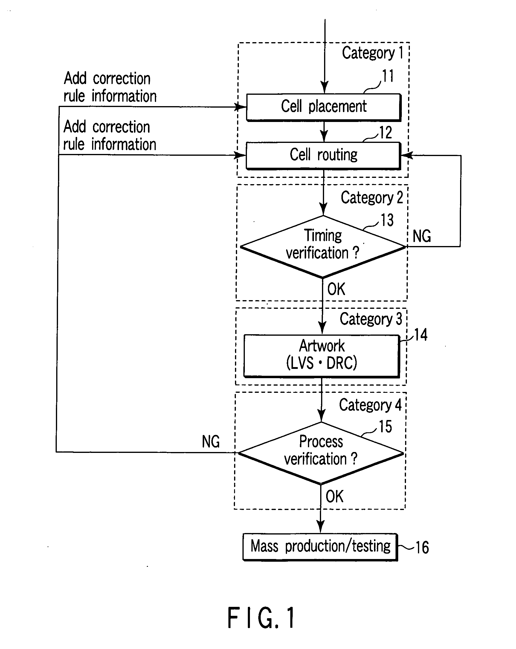
[0039]FIG. 1 is a flowchart showing a pattern data design method according to the first embodiment of the present invention.

[0040] In this embodiment, a cell placement step 11, cell routing step 12, timing verification step 13, artwork step 14, process verification step 15, and mass production / testing step 16 are executed sequentially. After the cell placement step 11 to process verification step 15, the verification result is fed back to the cell placement step 11 and cell routing step 12. In the conventional method, the cell placement step 11 to mass production / testing step 16 are executed continuously, as shown in FIG. 25. The first embodiment is different from the conventional method in this point.

[0041] In the conventional method, the continuous process is possible only when the layout has no problem from the viewpoint of both timing and lithography. Normally, since the layout has the above-described problems, the design pattern or mask pattern is repeatedly corrected until t...

second embodiment

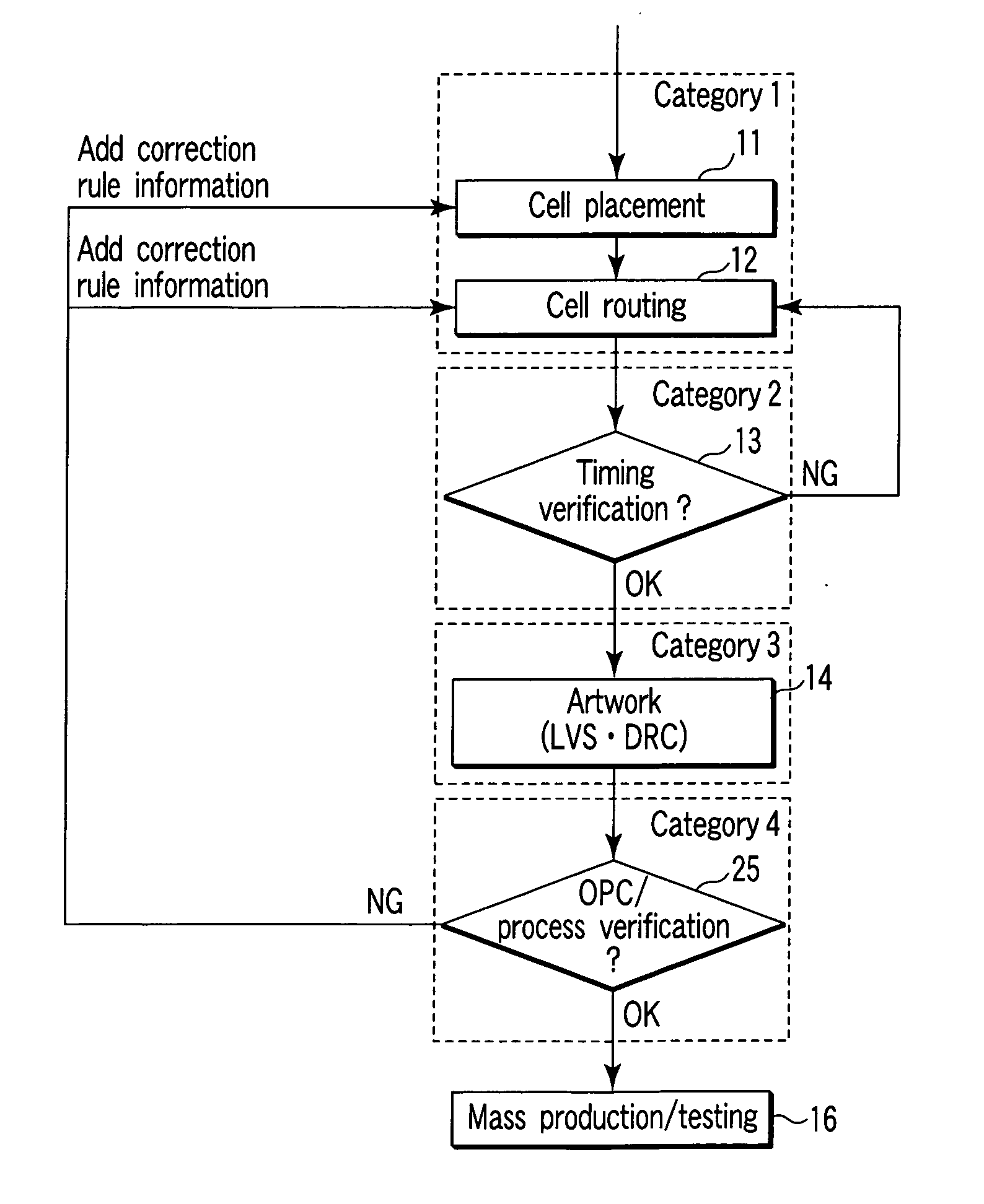
[0058]FIG. 7 is a flowchart showing a pattern data design method according to the second embodiment of the present invention.

[0059] The design flow of the second embodiment is almost the same as that of the first embodiment shown in FIG. 1 except that an OPC / process verification step 25 is executed in place of the process verification step 15. That is, the flow of this embodiment is different from that of the first embodiment in that an OPC process is executed for a design pattern in process verification of the step 25. The flow is different from the conventional method in that the result of the OPC / process verification step 25 is fed back to a cell placement step 11 or cell routing step 12. The process flow of this embodiment will be described below.

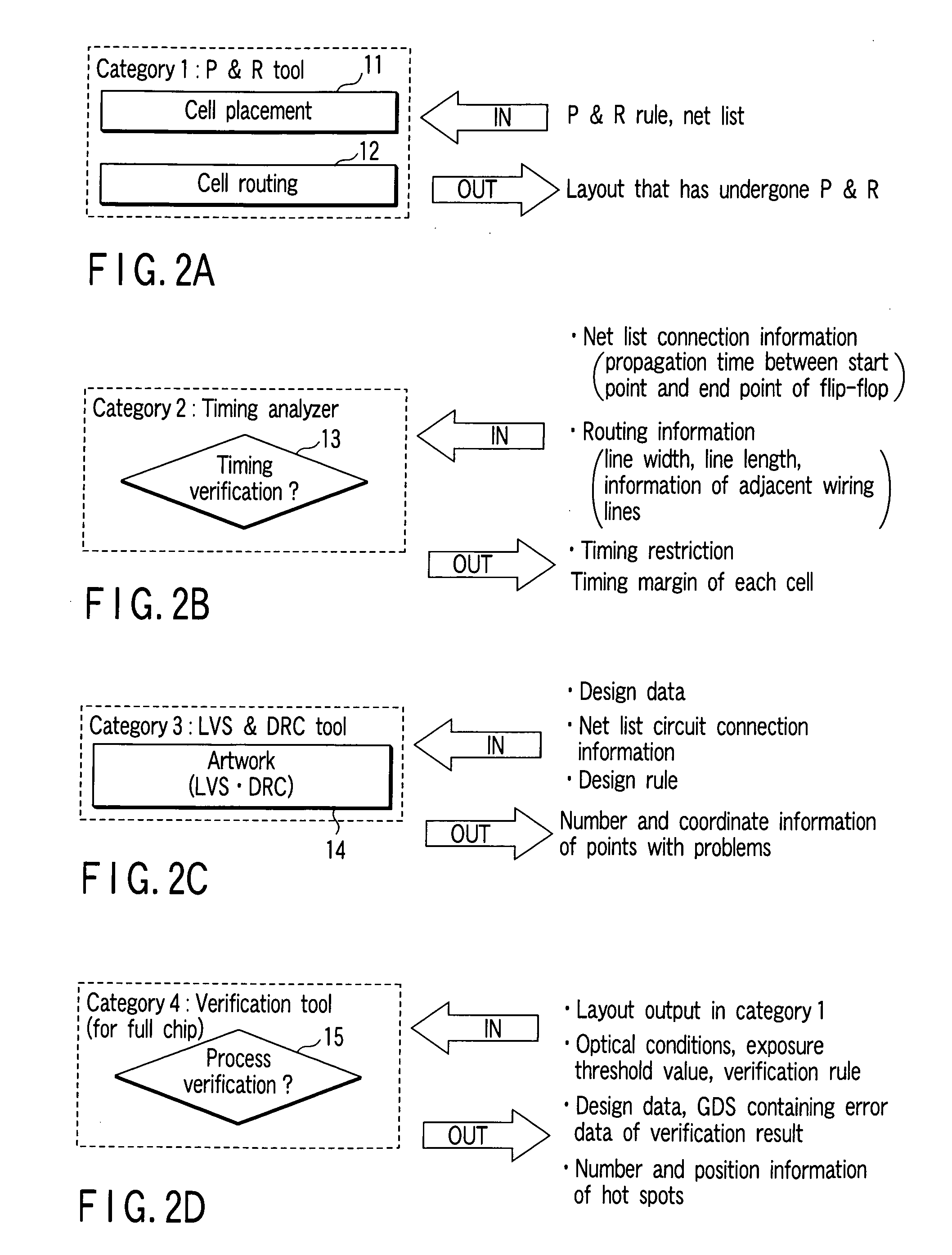
[0060]FIGS. 8A to 8D show categories of the flow in FIG. 7 divided in accordance with the tools of processes. As is apparent from comparison with FIGS. 2A to 2D, categories 1 to 3 in FIGS. 8A to 8C are the same as in the first embodim...

third embodiment

[0073]FIG. 9 is a flowchart showing a pattern data design method according to the third embodiment of the present invention.

[0074] The third embodiment is different from the first embodiment in that a critical path extraction step 31 is executed after a cell placement step 11 to timing verification step 13 of the first embodiment to selectively verify the area around the critical path. For this purpose, a critical path inclusive layout cutting step 32, local verification step 33, hot spot check step 34, layout correction method selection step 35, and incremental routing correction step 36 are added.

[0075]FIGS. 10A to 10D and 11A to 11C show categories of the flow in FIG. 9 divided in accordance with the tools of processes. In the process of this embodiment, as category 1 (steps 11 and 12), a cell placement / routing process is executed by using a P & R tool, as shown in FIG. 10A, as in the first embodiment. In category 2 (steps 13 and 31), as shown in FIG. 10B, timing verification i...


PUM

PropertyMeasurementUnit
widthaaaaaaaaaa
focal depthaaaaaaaaaa
electrical characteristicaaaaaaaaaa

Abstract

A semiconductor circuit pattern design method includes the following operations. A design pattern is created by placing a plurality of cells in each functional block as a unit of the semiconductor circuit and executing routing among the plurality of placed cells. Mask pattern data based on the design pattern is created. A predictive pattern to be formed on the substrate by the mask pattern data is predicted. A difference amount between the predictive pattern and a target pattern to be formed on the substrate by the mask pattern data is checked. The difference amount is compared with a predetermined allowable variation amount. If the difference amount is larger than the allowable variation amount in the comparison, at least one of placement and routing of the cells in the design pattern corresponding to the mask pattern data used to predict the predictive pattern is corrected.

Description

CROSS-REFERENCE TO RELATED APPLICATIONS [0001] This application is based upon and claims the benefit of priority from prior Japanese Patent Application No. 2005-137423, filed May 10, 2005, the entire contents of which are incorporated herein by reference. BACKGROUND OF THE INVENTION [0002] 1. Field of the Invention [0003] The present invention relates to a semiconductor circuit pattern design method for manufacturing a semiconductor device or liquid crystal display device, a computer program product for pattern design, and a method of manufacturing a semiconductor device or liquid crystal display device. [0004] 2. Description of the Related Art [0005] Along with the recent remarkable progress of semiconductor manufacturing technologies, semiconductor elements with a minimum line width of 0.1 μm or less have been mass-produced. This microfabrication is implemented by dramatic improvements of micropattern formation technologies and various EDA tools for circuit pattern generation. [00...

Claims


Application Information

Patent Timeline
Patent Type & Authority Applications(United States)
IPC IPC(8): G06F17/50G03F1/36G03F1/68G03F1/70G03F7/20H01L21/027H01L21/82
CPCG06F17/5031G06F17/5068G06F17/5036G06F30/3312G06F30/367G06F30/39
Inventor IZUHA, KYOKOMINAMI, FUMIHIROUEDA, TOSHIAKIOGAWA, RYUJITANAKA, SATOSHI
Owner KK TOSHIBA
Why Eureka
Try Eureka