Packaging of SMD light emitting diodes

a technology of light-emitting diodes and surface mount devices, which is applied in the direction of basic electric elements, semiconductor devices, electrical equipment, etc., can solve the problems of chromaticity change, permanent deformation, and very sensitive light output of led light sources, and achieve superior thermal dissipation capability and side-emitting characteristics, and easy mass production

Inactive Publication Date: 2006-12-28
IND TECH RES INST
View PDF14 Cites 9 Cited by
  • Summary
  • Abstract
  • Description
  • Claims
  • Application Information

AI Technical Summary

Benefits of technology

[0008] The present invention has been made to overcome the drawbacks of conventional LED light sources. The primary objective of the present invention is to provide an SMD LED package with superior thermal dissipation capability and side emitting characteristics using a low-cost mature manufacturing process for easy mass production.

Problems solved by technology

However, the light output of LED light sources is very sensitive to temperature, and in fact is permanently degraded by excessive temperature.
However, most commercially available LEDs are made with a limited number of chromaticity choices and their chromaticity may change over time.
However, all these schemes increase the complexity and cost of the light source.
Therefore, there is a limited flexibility for chromaticity adjustment.
The side-emitter may provide good uniformity of combined lights but the light intensity is poor.
In addition, these packaged LED chips normally occupy a large area.
This manufacturing process is not mature and the fragile silicon wafer may aggravate the poor manufacturing yield.

Method used


Image

  • Packaging of SMD light emitting diodes
  • Packaging of SMD light emitting diodes
  • Packaging of SMD light emitting diodes

Examples


Embodiment Construction

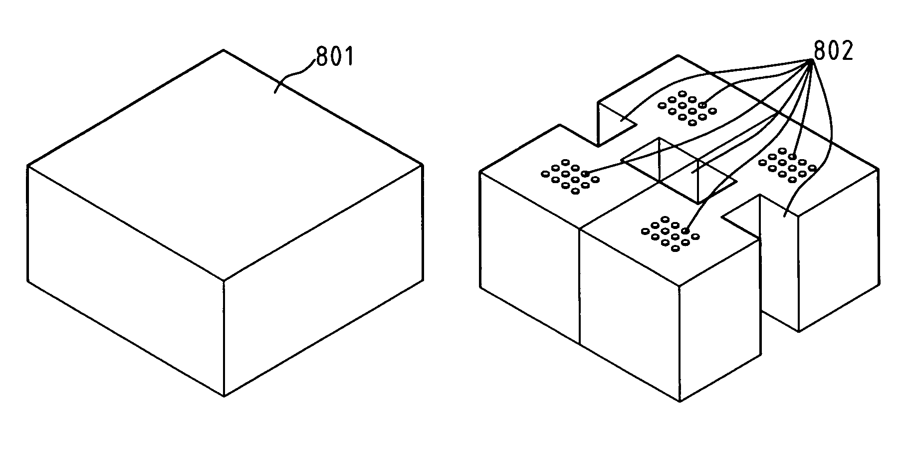
[0024]FIG. 5a shows a perspective view of an SMD LED package according to a preferred embodiment of the present invention. In the embodiment, the SMD LED package 500 comprises a supporting block 501 with circuit patterns and at least an LED chip 502 attached to the supporting block 501. The circuit patterns, which comprise an insulating layer 503 and conducting layer 504 for LED connection and SMD connection, are formed on and in the supporting block 501. The electrical connection of the LED chip 502 to the supporting block 501 can be obtained through metal bumps or bonding wires or some kinds of flip chip technology. And, the pattern design of the insulating layer 503 and the conducting layer 504 will be changed accordingly. These circuit patterns can be formed using conventional printed circuit board (PCB) or packaging process, such as printing, plating, sputtering, laser processing, etc.

[0025] Without loss of generality, only an LED chip is shown in FIG. 5a. FIG. 5b is a perspec...


PUM


Abstract

An SMD LED package with superior thermal dissipation capability is provided. The SMD LED package comprises a supporting block with circuit patterns and at least one LED attached to the supporting block. Wherein, circuit patterns of holes/vias, insulating layers, and conducting traces/pads are formed on and in the supporting block. The SMD LED packages can be further assembled to from a light module that allows emitted lights to travel in parallel with the mounting surface. The SMD manufacturing process is a mature production process and thus easy for mass production. Single or plural LED chips are mounted on a thermal conducting block that is disposed with patterns of conducting traces/pads and isolating dielectric layers. The side emitting characteristics of the present invention offers the advantage of reflecting and mixing the emitted lights to meet the desired chromaticity.

Description

FIELD OF THE INVENTION [0001] The present invention generally relates to the packaging of light emitting diodes (LEDs), and more specifically to the packaging of a surface mount device (SMD) LED that provides superior heat dissipation capability and side-emitting characteristics. BACKGROUND OF THE INVENTION [0002] LEDs have been proposed for use as light sources for many years. Recent developments of LED technology have expanded the use of LEDs from signs and message boards to automobile interior and exterior lights and traffic lights. However, the light output of LED light sources is very sensitive to temperature, and in fact is permanently degraded by excessive temperature. The aforementioned applications require that the substrate for the LEDs has a high heat dissipation capability, good heat-resistant property, and high mechanical strength. An LED light source with high heat dissipation capability to quickly carry away excessive heat is essential for maintaining its high perform...

Claims


Application Information

Patent Timeline
Patent Type & Authority Applications(United States)
IPC IPC(8): H01L33/00H01L33/48H01L33/62
CPCH01L33/486H01L33/62H01L2224/48227H01L2224/48247H01L2924/01078H01L2924/10253H01L2924/01079H01L2924/12041H01L2924/00
Inventor CHIANG, CHIA-WEN
Owner IND TECH RES INST
Why Eureka
Try Eureka