

Silicon film forming apparatus
a silicon film and apparatus technology, applied in the field of silicon film forming apparatus, can solve the problems of low film deposition rate, inability to meet the method and particularly the film deposition rate, and increase the production cost of silicon thin films, so as to improve the deposition rate for forming, the effect of smooth film formation and inexpensive form
- Summary
- Abstract
- Description
- Claims
- Application Information
AI Technical Summary
Benefits of technology
Problems solved by technology
Method used
Image

Examples
experimental example
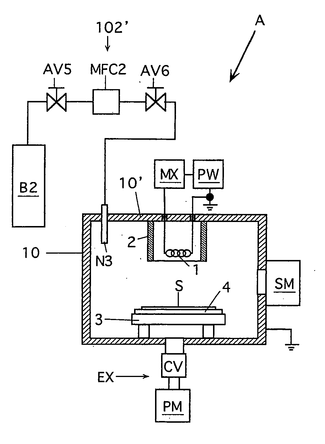
[0179] The deposition conditions are as follows:
[0180] High-frequency power: 60 MHz, 4000 W
[0181] Pressure and quantity of silane gas (SiH4) stored in gas reservoir unit GR [0182] Pressure: 0.07 MPa [0183] Quantity: 231 cc (selectable between 100 cc-300 cc)
[0184] Quantity of silane gas supplied by massflow controller MFC1: [0185] 1 sccm
[0186] Quantity of hydrogen gas supplied by massflow controller MFC2: [0187] 150 sccm
Deposition pressure: 0.67 Pa (5 mTorr)
[0188] Deposition chamber capacity: 1.5 m3
[0189] Deposition target substrate: non-alkali glass substrate
[0190] Substrate temperature: 400 deg. C. (400° C.)
[0191] Deposition film thickness: 500 angstroms (500 Å)
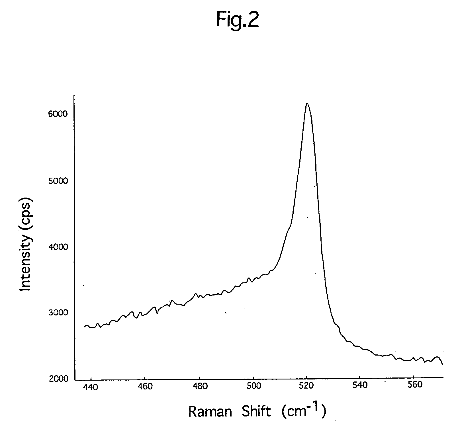
[0192] The silicon film was formed on the substrate under the above conditions, and a UV (ultraviolet ray) reflection side intensity in the interface between the film and the substrate and a UV reflection side intensity on the film surface were measured by the UV reflectance measurement. According to the result, t...
PUM
| Property | Measurement | Unit |
|---|---|---|
| wavelength | aaaaa | aaaaa |
| a wavelength | aaaaa | aaaaa |
| wavelength | aaaaa | aaaaa |
Abstract
Description
Claims
Application Information