Uniform batch film deposition process and films so produced

Inactive Publication Date: 2007-01-11
AVIZA TECHNOLOGY INC
View PDF13 Cites 429 Cited by
  • Summary
  • Abstract
  • Description
  • Claims
  • Application Information

AI Technical Summary

Benefits of technology

[0013] A batch of wafer substrates is provided with each wafer substrate having a surface. Each surface is coated with a layer of material applied simultaneously to the surface of each of the batch of wafer substrates. The layer of material is applied to a thickness that varies less than four thickness percent across the surface and exclusive of an edge boundary and having a wafer-to-wafe

Problems solved by technology

In addition to high deposition temperatures associated with conventional batch process chemical vapor deposition, there is a growing appreciation that contaminants associated with these processes limit the effectiveness of the deposited materials to perform as intended barrier or insulative layers.
By way of example, the use of a chlorinated silane precursor or co-reactant leads to chlorine incorporation into a deposited layer to the detriment of the material performance.
Unfortunately, these precursors have met with limited acceptance owing to coking during material deposition.
These problems associated with chlorine and carbon inclusion have led to the exploration of various silylamines.
Silylamines tend to incorporate hydrogen as an impurity that migrates readily and diminishes material performance.
While deposition of silicon nitride and silicon oxynitri

Method used


Image

  • Uniform batch film deposition process and films so produced
  • Uniform batch film deposition process and films so produced
  • Uniform batch film deposition process and films so produced

Examples


example 1

[0086] A batch of 20 wafers was dispersed along a 120 wafer carrier with substrate blanks filling the unused 100 positions. After stabilizing a wafer substrate temperature and an inert dinitrogen atmosphere, trisilylamine and ammonia gas are introduced into the reactor at flow rates of 15 and 225 sccm while the reactor total pressure is maintained at 3 Torr with a controlled flow of argon gas. The deposition is allowed to proceed for 30 minutes at a reaction temperature of 515° C. A deposition rate of 1.8 Angstroms per minute is noted. WIW uniformity for the resultant silicon nitride film is 2.3 thickness percent (three sigma) while WTW thickness variation is 2.6 percent. Auger spectroscopy indicated the resultant deposited layer of material to be devoid of carbon and chlorine and having less than 8 atomic percent substitution hydrogen for the silicon counterions.

examples 2-6

[0087] The process of Example 1 is repeated with a change in wafer substrate temperature. Comparable uniformity to that of Example 1 is noted while variations in deposition rate as a function of temperature are provided in Table 2 along with the comparative temperature and deposition rates for prior art precursors. Auger spectroscopy indicated the resultant deposited layer of material to be devoid of carbon and chlorine and having less than 10 atomic percent substitution hydrogen for the silicon counterions.

TABLE 2Batch SiN Layer Deposition as a Function of TemperatureSubstrate Temp.Deposition RateExamplePrecursor(° C.)(Å / mm)1trisilylamine / NH35151.82trisilylamine / NH35254.03trisilylamine / NH35409.34trisilylamine / NH355010.35trisilylamine / NH3575136trisilylamine / NH360018Comp. Adichlorosilane / NH375017.3Comp. Bbis t-butylamino57010.0silane / NH3

example 7

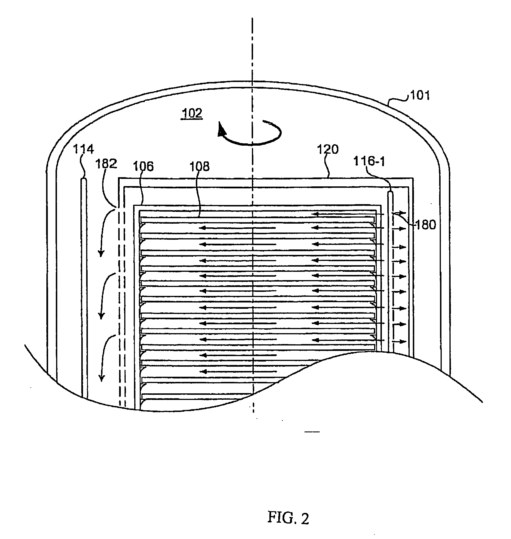
[0088] A low temperature oxide material layer is deposited with the reactor according to FIG. 1 with the reactor maintained at a total pressure of 7 Torr with dinitrogen as an inert gas, trisilylamine and oxygen being metered into the reactor at rates of 11 and 200 sccm, respectively. The nitrogen flow rate is approximately 500 sccm. The deposition rate and WIW nonuniformity (one sigma) as a function of deposition temperature between 200°0 and 450° C. is provided in FIG. 6. WTW variation is less than 3%. Auger spectroscopy indicated the resultant deposited layer of material to be devoid of carbon and chlorine and having less than 10 atomic percent substitution hydrogen for the silicon counterions.


PUM

PropertyMeasurementUnit
Fractionaaaaaaaaaa
Pressureaaaaaaaaaa
Pressureaaaaaaaaaa

Abstract

A batch of wafer substrates is provided with each wafer substrate having a surface. Each surface is coated with a layer of material applied simultaneously to the surface of each of the batch of wafer substrates. The layer of material is applied to a thickness that varies less than four thickness percent across the surface and exclusive of an edge boundary and having a wafer-to-wafer thickness variation of less than three percent. The layer of material so applied is a silicon oxide, silicon nitride or silicon oxynitride with the layer of material being devoid of carbon and chlorine. Formation of silicon oxide or a silicon oxynitride requires the inclusion of a co-reactant. Silicon nitride is also formed with the inclusion of a nitrification co-reactant. A process for forming such a batch of wafer substrates involves feeding the precursor into a reactor containing a batch of wafer substrates and reacting the precursor at a wafer substrate temperature, total pressure, and precursor flow rate sufficient to create such a layer of material. The delivery of a precursor and co-reactant as needed through vertical tube injectors having multiple orifices with at least one orifice in registry with each of the batch of wafer substrates and exit slits within the reactor to create flow across the surface of each of the wafer substrates in the batch provides the within-wafer and wafer-to-wafer uniformity.

Description

RELATED APPLICATION [0001] This application claims priority of U.S. Provisional Patent Application Ser. No. 60 / 697,784 filed Jul. 9, 2005, which is incorporated herein by reference.FIELD OF THE INVENTION [0002] The present invention relates generally to depositing a layer of silicon-nitrogen, silicon-oxygen, or silicon-nitrogen-oxygen material simultaneously on a plurality of substrates and in particular to the use of a silylamine precursor in combination with a across-flow liner to achieve a degree of within-wafer and wafer-to-wafer uniformity while improving impurity profiles to form silicon-oxygen, silicon-nitrogen, or silicon-nitrogen-oxygen materials. BACKGROUND OF THE INVENTION [0003] Thermal processing apparatuses are commonly used in the manufacture of integrated circuits (ICs) or semiconductor devices from semiconductor substrates or wafers. Thermal processing of semiconductor wafers include, for example, heat treating, annealing, diffusion or driving of dopant material, de...

Claims


Application Information

Patent Timeline
IPC IPC(8): H01L21/20
CPCC23C16/308H01L21/3185C23C16/402C23C16/45504C23C16/45578C23C16/54H01L21/0214H01L21/02164H01L21/0217H01L21/02222H01L21/02271H01L21/02274H01L21/3145H01L21/31612C23C16/345H01L21/00H01L21/20H01L21/324H01L21/477
Inventor BAILEY, ROBERT JEFFREYQIU, TAIQING T.PORTER, COLELAPARRA, OLIVIERCHATHAM, ROBERT H.MOGAARD, MARTINTREICHEL, HELMUTH
Owner AVIZA TECHNOLOGY INC
Why Eureka
Try Eureka