Method of Surface Treating Substrates and Method of Manufacturing III-V Compound Semiconductors

a surface treatment and semiconductor technology, applied in the direction of packaging foodstuffs, pharmaceutical containers, packaged goods types, etc., can solve the problems of high cost, high cost, and high cost, and achieve the effect of reducing haze, reducing micro-roughness of the surface, and improving cleaning ability

Inactive Publication Date: 2007-01-18
SUMITOMO ELECTRIC IND LTD
View PDF3 Cites 16 Cited by
  • Summary
  • Abstract
  • Description
  • Claims
  • Application Information

AI Technical Summary

Benefits of technology

[0025] Accordingly, a Group III-V compound semiconductor is manufactured in which the substrate surface is stoichiometric and the microscopic roughness of the surface is reduced.
[0026] According to the present invention, since pH of the cleaning solution is ...

Problems solved by technology

However, if the typical surface treatment method by an ozonated water process disclosed in Pat. App. Pub. No. 2001-189278 is applied to InP, the surface roughness of InP does not decrease.
As a result, in epitaxial growth the surface is likely to become roughened because Group III oxide hinders epitaxial growth.
With the generation of a dense oxide on the Ga surface, it is likely to become roughened when an epitaxial film is grown on the surface, because the oxide hinders the epitaxial growth.
Consequently, dense Group V oxide is generated on the surface and hinders epitaxial growth.
The overly high concentration of the aqueous hydrogen peroxide...

Method used


Image

  • Method of Surface Treating Substrates and Method of Manufacturing III-V Compound Semiconductors
  • Method of Surface Treating Substrates and Method of Manufacturing III-V Compound Semiconductors
  • Method of Surface Treating Substrates and Method of Manufacturing III-V Compound Semiconductors

Examples


embodiment 1

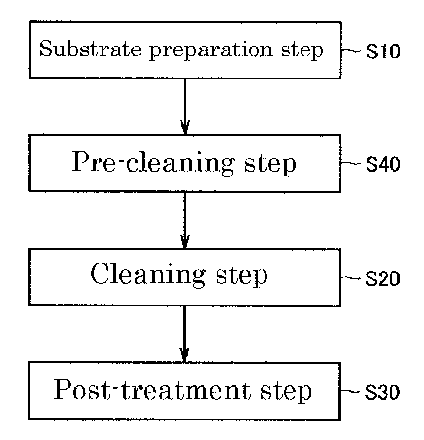
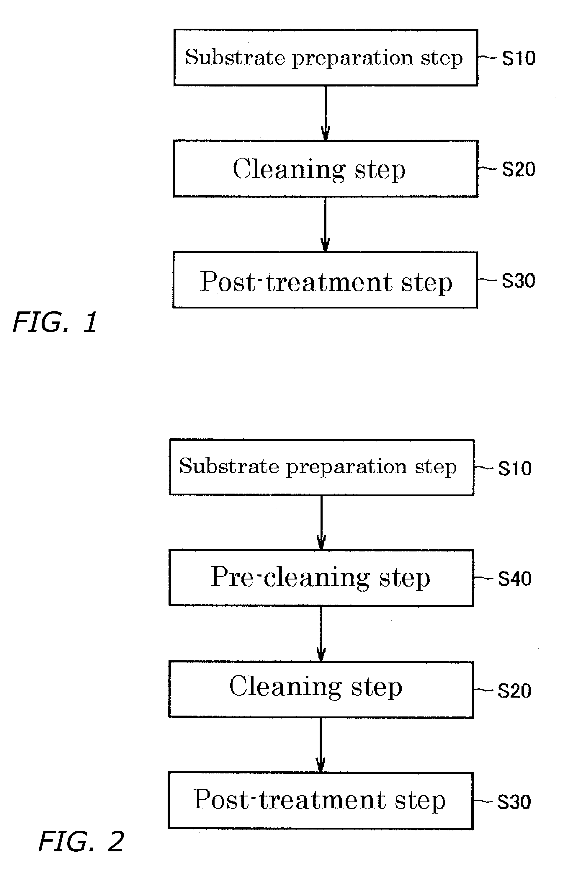
[0033]FIG. 1 is a flow chart showing a method of surface treating a substrate in Embodiment 1 of the present invention. Referring to FIG. 1, the substrate surface treating method in Embodiment 1 of the present invention will be described.

[0034] As shown in FIG. 1, a substrate preparation step (S10) is performed first in the substrate surface treating method in Embodiment 1, in which a substrate composed of Group III-V compound is prepared. The prepared substrate may be a bulk crystal or a thin film formed on a substrate made of a bulk crystal, for example.

[0035] Next, a cleaning step (S20) is performed. In the cleaning step (S20), the substrate is cleaned with a cleaning solution whose pH has been adjusted to be acidic from 2 to 6.3 inclusive and to which an oxidizing agent has been added. It is preferable that as the cleaning solution a cleaning solution composed of DI water (a cleaning solution composed of DI water in which pH has been adjusted to be acidic from 2 to 6.3 inclusi...

embodiment 2

[0043]FIG. 2 is a flow chart that shows a substrate surface treating method in Embodiment 2 of the present invention. Referring to FIG. 2, the substrate surface treating method in Embodiment 2 of the present invention will be described.

[0044] As shown in FIG. 2, the substrate surface treating method (cleaning method) in Embodiment 2 has basically steps similar to those of the substrate surface treating method in Embodiment 1 of the present invention.

[0045] More specifically, in a pre-cleaning step (S40), before the cleaning step (S20), the substrate is cleaned with an alkaline cleaning solution. The pre-cleaning step (S40) may include a chemical cleaning step, a rinsing step (DI water rinsing step), and a drying step. The chemical cleaning step and the rinsing step (DI water rinsing step) can be repeated several times, if necessary.

[0046] In the pre-cleaning step (S40), in order to remove impurities from the surface of the substrate composed of Group III-V compound semiconductor,...

embodiment 3

[0048] Referring to FIG. 2, a substrate surface treating method in Embodiment 3 of the present invention will be described. As shown in FIG. 2, the substrate surface treating method (cleaning method) in Embodiment 3 has basically steps similar to those of the substrate surface treating method in Embodiment 2 of the present invention.

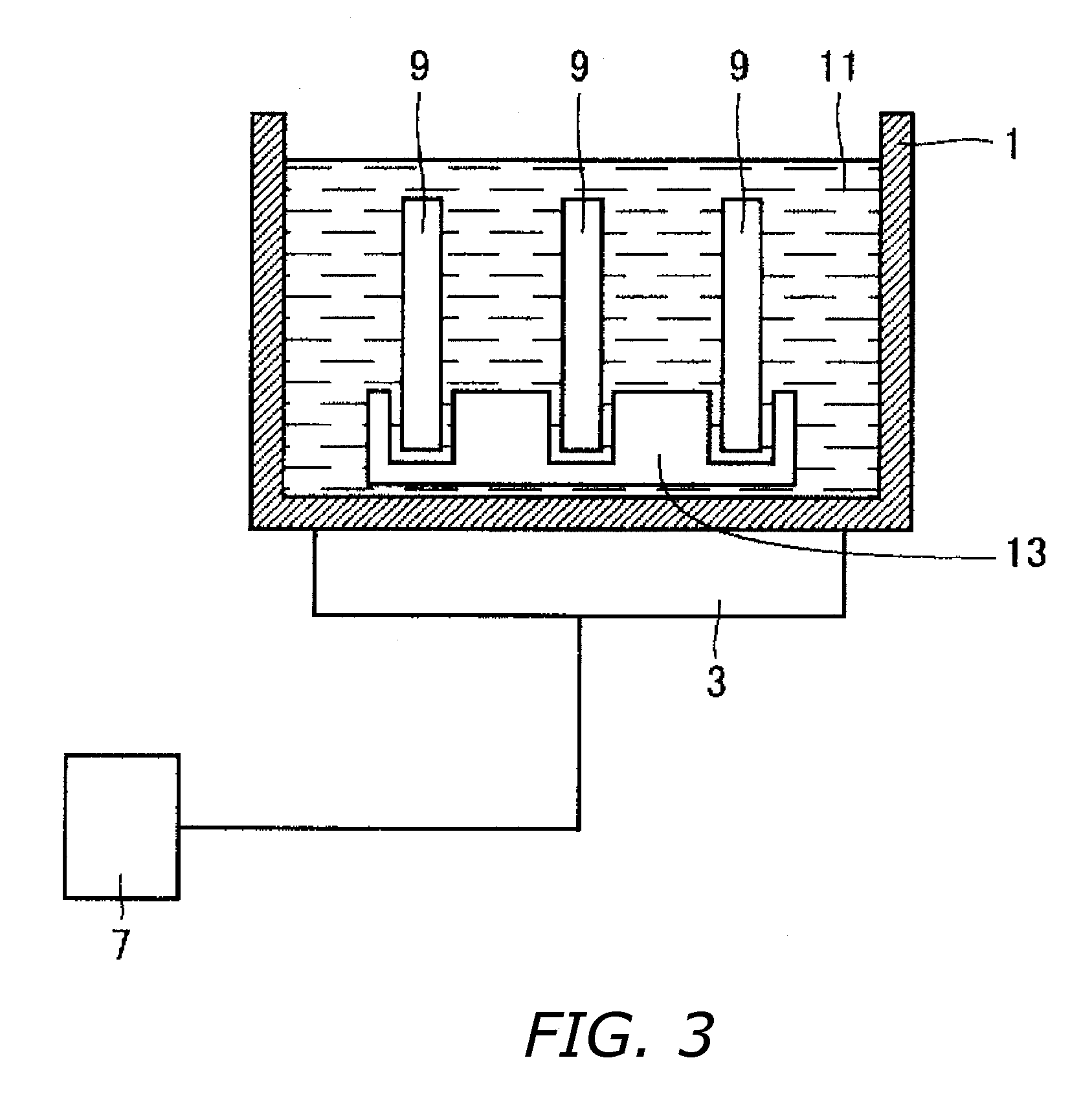
[0049] Specifically, the cleaning step (S20) includes a rinse step of cleaning the substrate with DI water to which ultrasonic wave is being applied. In the rinse step, vibrations or shaking is applied to the cleaning solution using a ultrasonic device, as shown in FIG. 3, for example.

[0050] More specifically, the cleaning step (S20) may include a chemical cleaning step, a rinse step, and a drying step. The chemical cleaning step and the rinse step can be repeated several times, if required.

[0051]FIG. 3 is a schematic cross sectional view of showing a processing apparatus used for the rinse step. Referring to FIG. 3, the processing apparatus used for ...


PUM


Abstract

Affords methods of surface treating a substrate and of manufacturing Group III-V compound semiconductors, in which a substrate made of a Group III-V semiconductor compound is rendered stoichiometric, and microscopic roughness on the surface following epitaxial growth is reduced. The methods include preparing a substrate made of a Group III-V semiconductor compound (S10), and cleaning the substrate with a cleaning solution whose pH has been adjusted to an acidity of 2 to 6.3 inclusive, and to which an oxidizing agent has been added (S20).

Description

BACKGROUND OF THE INVENTION [0001] 1 Technical Field [0002] The present invention relates to methods of surface treating substrates and to methods of manufacturing (Group) III-V compound semiconductors; in particular the invention relates to substrate surface treating and III-V compound semiconductor manufacturing methods that enable the reduction of post-epitaxial-growth surface roughness. [0003] 2 Description of the Related Art [0004] Substrates composed of Group III-V semiconductor compounds have been widely used for semiconductor lasers, LEDs, and high-speed devices because they have luminescent properties and high electron mobility. Surface treatment is typically carried out in methods of manufacturing substrates composed of Group III-V semiconductor compounds. Such surface treatments include, for example, the surface treatment method disclosed in Japanese Unexamined Pat. App. Pub. No. 2001-189278, and the method of cleaning an InP wafer disclosed in Japanese Unexamined Pat. Ap...

Claims


Application Information

Patent Timeline
IPC IPC(8): A61L33/00H01L21/205H01L21/304H01L21/308
CPCH01L21/02052Y10S438/906H01L21/304H01L31/0304
Inventor NISHIURA, TAKAYUKIUEMURA, TOMOKI
Owner SUMITOMO ELECTRIC IND LTD
Why Eureka
Try Eureka