Switch mode power amplifier using MIS-HEMT with field plate extension

Active Publication Date: 2007-01-25
CREE INC
View PDF8 Cites 182 Cited by
  • Summary
  • Abstract
  • Description
  • Claims
  • Application Information

AI Technical Summary

Benefits of technology

[0008] The invention is directed to a field effect transistor which can be used i

Problems solved by technology

In practice, this is difficult to realize due to the very large forward currents that

Method used


Image

  • Switch mode power amplifier using MIS-HEMT with field plate extension
  • Switch mode power amplifier using MIS-HEMT with field plate extension
  • Switch mode power amplifier using MIS-HEMT with field plate extension

Examples


Example

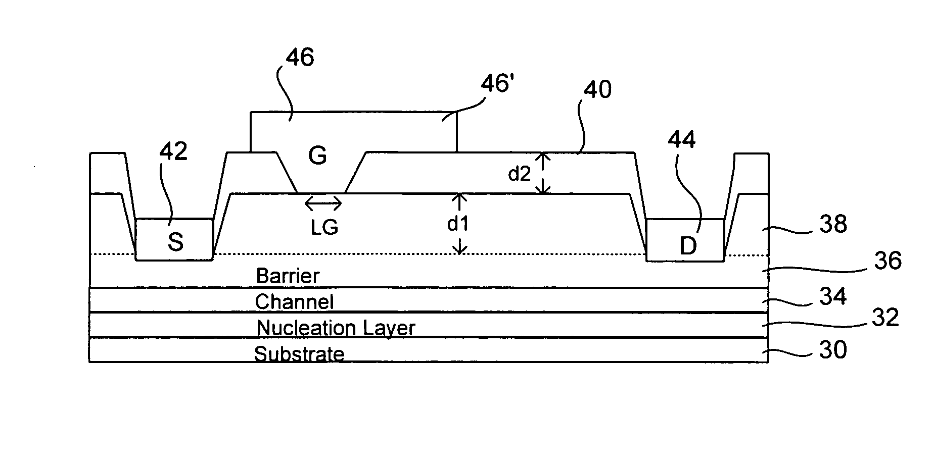
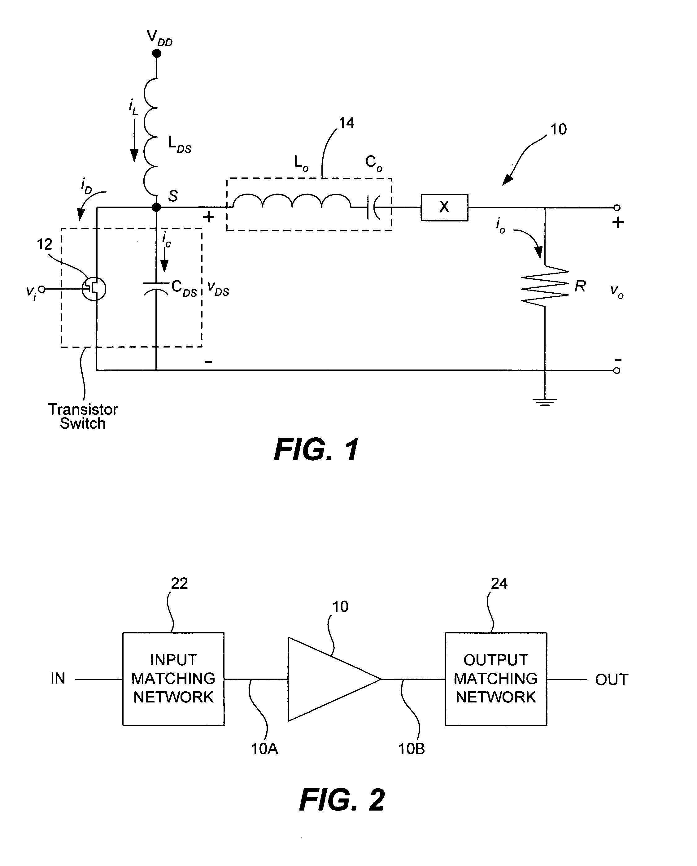
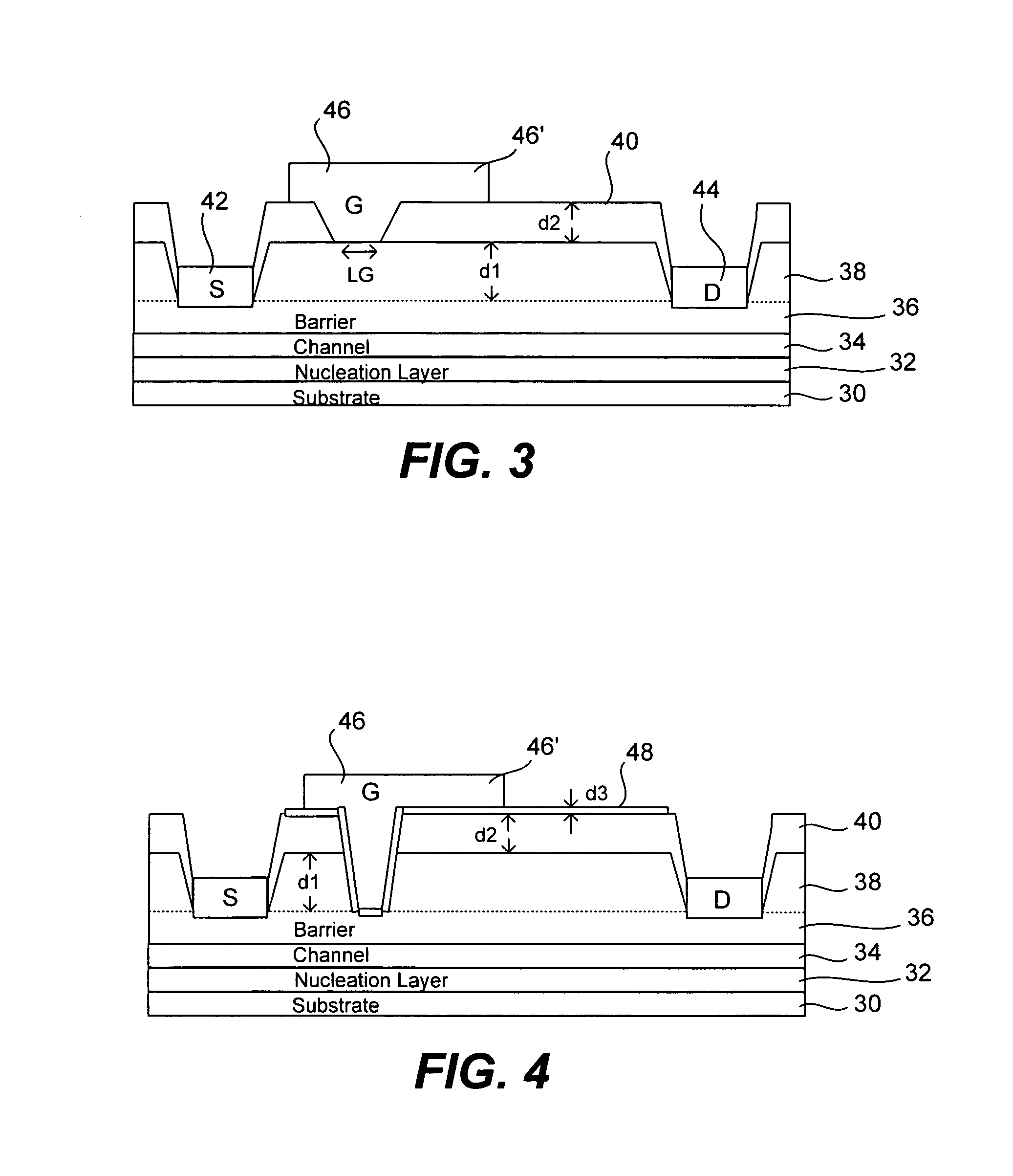
[0017] Referring now to FIG. 1, a single-stage switch mode power amplifier circuit model 10 in accordance with an embodiment of the invention is illustrated. Amplifier 10 includes a metal-insulator-semiconductor transistor 12 comprising a wide bandgap transistor which functions as an on / off switch. The use of an insulator separating the gate from the semiconductor body limits forward conduction from gate to source under high stress drive, in some embodiments. The transistor 12 comprises a GaN HEMT. Transistor 12 may alternatively comprise a different wide bandgap high-frequency transistor, such as a SiC MESFET, GaN MESFET, SiC LDMOS, SiC bipolar transistor, or GaN MOSHFET device.

[0018] An input voltage signal vi is applied to the gate of transistor 12, which controls the state of the transistor 12. The input voltage signal vi is biased close to the pinch-off voltage of the transistor 12. The drain of the transistor 12 is coupled to an output node S, and the source of transistor 12 ...


PUM


Abstract

Disclosed are a switch mode power amplifier and a field effect transistor especially suitable for use in a switch mode power amplifier. The transistor is preferably a compound high electron mobility transistor (HEMT) having a source terminal and a drain terminal with a gate terminal therebetween and positioned on a dielectric material. A field plate extends from the gate terminal over at least two layers of dielectric material towards the drain. The dielectric layers preferably comprise silicon oxide and silicon nitride. A third layer of silicon oxide can be provided with the layer of silicon nitride being positioned between layers of silicon oxide. Etch selectivity is utilized in etching recesses for the gate terminal.

Description

CROSS REFERENCE TO RELATED APPLICATIONS [0001] This application is related to co-pending application Ser. No. 11 / 132,619, assigned to the present assignee, which is incorporated herein by reference for all purposes. This application is related to the following co-pending applications: U.S. Patent Publication No. US20050051796A1, entitled “WIDE BANDGAP TRANSISTOR DEVICES WITH FIELD PLATES”; U.S. Patent Publication No. US20050051800A1, entitled “CASCODE AMPLIFIER STRUCTURES INCLUDING WIDE BAND GAP FIELD EFFECT TRANSISTOR WITH FIELD PLATE”; U.S. patent application Ser. No. 10 / 958,970, filed Oct. 4, 2004, entitled “WIDE BAND GAP FIELD EFFECT TRANSISTORS WITH FIELD PLATES”; U.S. patent application Ser. No. 10 / 976,422, filed Oct. 29, 2004, entitled “WIDE BAND GAP FIELD EFFECT TRANSISTOR WITH DUAL FIELD PLATES”; U.S. patent application Ser. No. 10 / 958,945, filed Oct. 4, 2004, entitled “WIDE BAND GAP FIELD EFFECT TRANSISTORS WITH SOURCE CONNECTED FIELD PLATES”; and U.S. patent application S...

Claims


Application Information

Patent Timeline
IPC IPC(8): H01L29/76
CPCH01L29/2003H01L29/267H01L29/402H01L29/42368H01L29/42376H01L21/28264H01L29/518H01L29/7787H03F3/189H03F3/217H03F3/2176H01L29/513H01L29/76
Inventor SHEPPARD, SCOTT
Owner CREE INC
Why Eureka
Try Eureka