Semiconductor device and method for fabricating the same

a technology of semiconductor devices and electrodes, applied in the direction of semiconductor devices, basic electric elements, electrical equipment, etc., can solve the problems of insufficient reduction of the value of the source-to-gate resistance value, difficulty in forming a gate electrode on the bottom surface of the recess, and difficulty in wet etching, so as to reduce the surface potential of electrons, reduce the source resistance, and improve the drain current value

Inactive Publication Date: 2007-01-25
PANASONIC CORP
View PDF7 Cites 4 Cited by
  • Summary
  • Abstract
  • Description
  • Claims
  • Application Information

AI Technical Summary

Benefits of technology

[0011] The present invention has been achieved in view of the foregoing problems and it is therefore an object of the present invention to reduce a surface potential for electrons in a group III-V nitride semiconductor and thereby reduce a source resistance, improve a drain current value, and increase a drain breakdown voltage.
[0013] Since the first method for fabricating a semiconductor device selectively forms the ohmic electrode and the gate electrode on the active region with the reduced surface potential, a source resistance is reduced and a transconductance is increased. This advantageously increases a drain current as well as a drain breakdown voltage.
[0015] A second method for fabricating a semiconductor device according to the present invention comprises the steps of: (a) selectively forming an ohmic electrode and a gate electrode on an active region composed of a group III-V nitride semiconductor; and (b) exposing the active region to a plasma by using the ohmic electrode and the gate electrode as a mask to reduce a surface potential for an electron in an exposed region of the active region.
[0018] In the first semiconductor device, a source resistance is reduced and a transconductance is increased so that a drain current is increased advantageously.
[0020] This also reduces a drain resistance so that the drain current is further increased.
[0022] In the second semiconductor device, a source resistance is reduced and a drain current is increased advantageously, while a gate-to-drain breakdown voltage is also increased advantageously.

Problems solved by technology

However, the FET having a GaN heterojunction structure has the problem that it is difficult to form a gate electrode on the bottom surface of a recess provided in the upper semiconductor thereof, i.e., a so-called recessed gate structure.
The reasons for this is that AlGaN and GaN in, e.g., an AlGaN / GaN heterojunction structure have different lattice constants and therefore an upper semiconductor layer composed of AlGaN cannot be formed sufficiently thick on a lower semiconductor layer composed of GaN and that wet etching is difficult because AlGaN is a chemically extremely stable material.
Thus, in the structure in which the individual electrodes are formed on the same surface, it is difficult to sufficiently reduce the value of a source-to-gate resistance so that excellent physical properties inherent to the materials composing the GaN-based heterojunction structure FET cannot be obtained.
However, the use of a recessed gate structure in a FET having a GaN-based heterojunction structure is technically difficult, as described above, so that it is necessary to minimize the surface potential between the source and drain.

Method used


Image

  • Semiconductor device and method for fabricating the same
  • Semiconductor device and method for fabricating the same
  • Semiconductor device and method for fabricating the same

Examples


embodiment 1

[0043] A first embodiment of the present invention will be described with reference to the drawings.

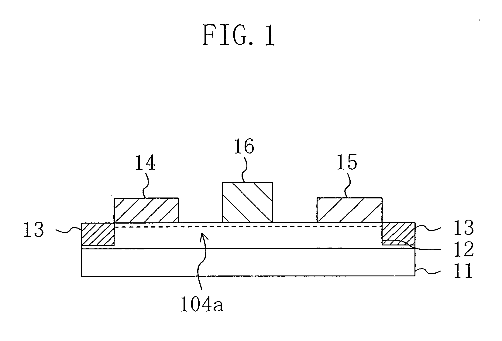
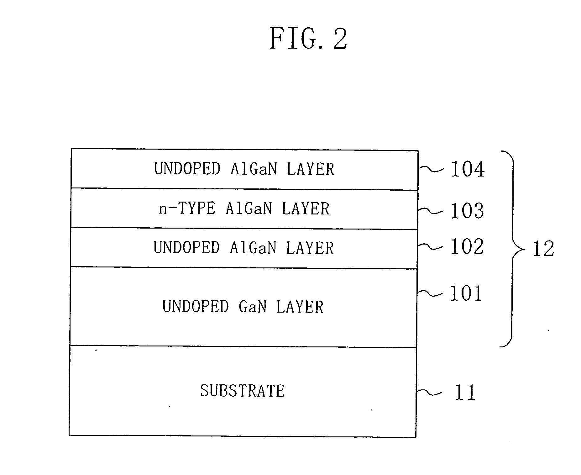
[0044]FIG. 1 shows a cross-sectional structure of a MESFET (Metal Semiconductor FET) as a semiconductor device according to the first embodiment. As shown in FIG. 1, an epitaxial layer 12 composed of a GaN-based semiconductor is formed on a substrate 11 composed of, e.g., sapphire. An isolation region 13 for defining the active region of the transistor is formed in the epitaxial layer 12.

[0045] The isolation region may be formed by implanting nitrogen (N) ions or carbon (C) ions or by selectively oxidizing the epitaxial layer 12.

[0046] A source electrode 14 and a drain electrode 15 are formed as ohmic electrodes on the both end portions of the epitaxial layer 12 on the active region. A gate electrode 16 composed of metal is formed on the center portion of the active region in spaced apart relation to the source electrode 14 and the drain electrode 15.

[0047] The first embodiment is...

embodiment 2

[0063] A second embodiment of the present invention will be described with reference to the drawings.

[0064]FIG. 6 shows a cross-sectional structure of a MESFET as a semiconductor device according to the second embodiment. The description of the components which are shown in FIG. 6 and also shown in FIG. 1 will be omitted by retaining the same reference numerals.

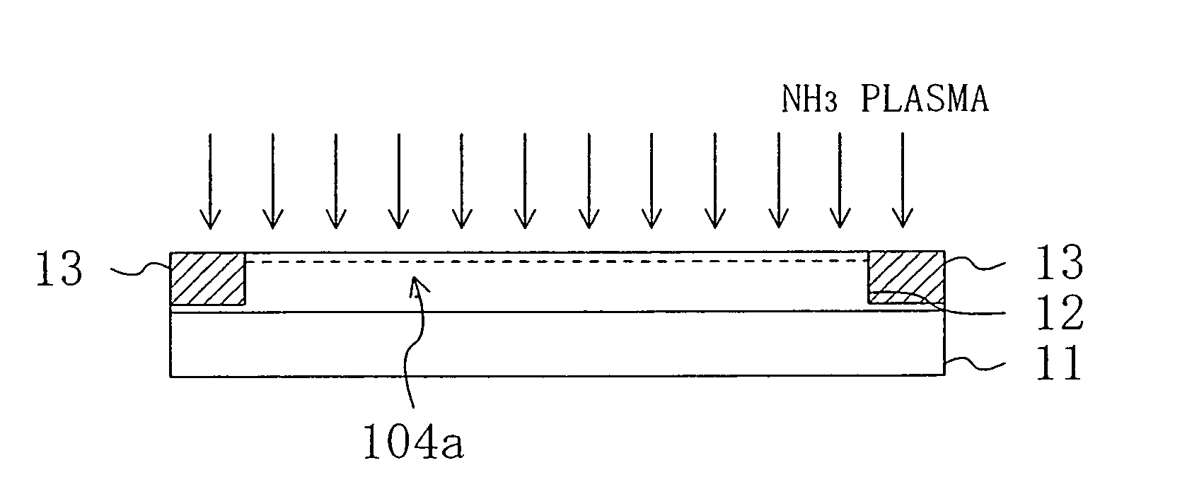
[0065] The second embodiment is characterized in that a modified layer 104a obtained by exposing the surface of the epitaxial layer 12 to an ammonia plasma is formed selectively in the surface region of an epitaxial layer 12 located between a source electrode 14 and a gate electrode 16. A material composing the substrate 11 is not limited to sapphire. Silicon carbide (SiC) may also be used instead.

[0066] A description will be given herein below to a method for fabricating the MESFET thus constructed with reference to the drawings.

[0067]FIGS. 7A to 7C show respective cross-sectional structures of the MESFET according to th...

embodiment 3

[0074] A third embodiment of the present invention will be described with reference to the drawings.

[0075]FIG. 8 shows a cross-sectional structure of a MESFET as a semiconductor device according to the third embodiment. The description of the components which are shown in FIG. 8 and also shown in FIG. 6 will be omitted by retaining the same reference numerals.

[0076] The third embodiment is characterized in that a modified layer 104a obtained by exposing the surface of an epitaxial layer 12 to an ammonia plasma is formed in each of the respective surface regions of the epitaxial layer 12 located between a source electrode 14 and a gate electrode 16 and between the gate electrode 16 and a drain electrode 15. A material composing the substrate 11 is not limited to sapphire. Silicon carbide (SiC) may also be used instead.

[0077] The structure reduces a threshold voltage in each of the regions located between the source and gate and the gate and drain by a value as large as about 10 V,...


PUM


Abstract

A semiconductor device has an active region composed of a group III-V nitride semiconductor and ohmic electrodes and a gate electrode each formed on the active region. The active region has an entire surface thereof exposed to a plasma such that a surface potential for electrons therein is lower than in the case where the entire surface is not exposed to the plasma.

Description

BACKGROUND OF THE INVENTION [0001] The present invention relates to a semiconductor device composed of a group III-V nitride semiconductor represented by a general formula (InXAl1-X)YGa1-YN (where 0≦X≦1 and 0≦Y≦1 are satisfied) and to a method for fabricating the same. [0002] A group III-V nitride semiconductor such as GaN, AlGaN, InGaN, or InAlGaN, i.e., a so-called gallium nitride-based semiconductor is an important semiconductor for an optical device having a short oscillating wavelength such as a semiconductor laser device outputting, e.g., a blue laser beam. The applications of the gallium nitride-based semiconductor are not limited to the optical device. In recent years, attention has been focused on the gallium nitride-based semiconductor for its high dielectric breakdown field strength, high thermal conductivity, and high electron saturation velocity so that gallium nitride-based semiconductor is considered to be promising also as the material of an RF power device. [0003] I...

Claims


Application Information

Patent Timeline
Patent Type & Authority Applications(United States)
IPC IPC(8): H01L21/26H01L21/28H01L21/338H01L29/20H01L29/778H01L29/812
CPCH01L21/28575H01L29/2003H01L29/8126H01L29/66462H01L29/66878H01L29/452
Inventor INOUE, KAORUIKEDA, YOSHITOHIROSE, YUTAKANISHII, KATSUNORI
Owner PANASONIC CORP
Why Eureka
Try Eureka