Electron emission source, method of preparing the same, and electron emission device employing the electron emission source

a technology of electron emission source and electron emission device, which is applied in the manufacture of electrode systems, electric discharge tubes/lamps, and discharge tubes luminescnet screens, etc., can solve the problems of adversely affecting the lifespan of electron emission devices and deterioration of electron emission sources, and achieve the effect of improving reliability and long li

Inactive Publication Date: 2007-02-01
SAMSUNG SDI CO LTD
View PDF2 Cites 12 Cited by
  • Summary
  • Abstract
  • Description
  • Claims
  • Application Information

AI Technical Summary

Benefits of technology

[0010] The present invention provides an electron emission source having long lifespan without deterioration of electron emitting characteristics, a method of preparing the same, and an electron emission device employing the electron emission source to have improved reliability.

Problems solved by technology

Due to this, the carbon nanotubes react with oxygen in electron emission devices during driving the devices, resulting in deterioration of electron emission sources.
This adversely affects the lifespan of electron emission devices.

Method used


Image

  • Electron emission source, method of preparing the same, and electron emission device employing the electron emission source
  • Electron emission source, method of preparing the same, and electron emission device employing the electron emission source
  • Electron emission source, method of preparing the same, and electron emission device employing the electron emission source

Examples


synthesis example 1

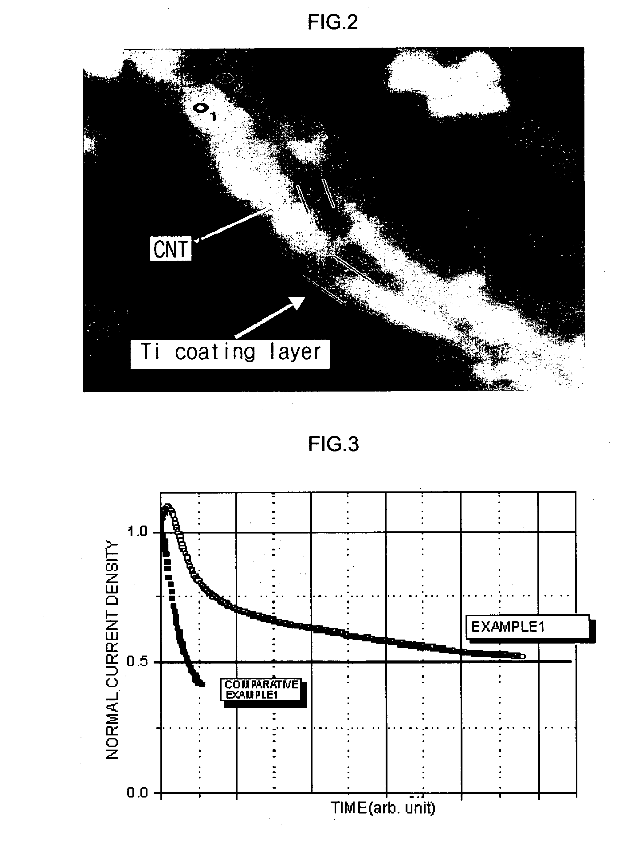
[0061] Ti was coated on CNT (MWNT, available from ILJIN Nanotech Co., Ltd) using a solution coating method to form a 10 nm thick Ti coating layer. FIG. 2 is a scanning transmission electron microscopic (STEM) image of the CNT having the Ti coating layer.

preparation example 1

[0062] 1 g of the CNT prepared in the Synthesis Example 1, 5 g of polyester acrylate, and 5 g of benzophenone were added into 10 g of terpineol and stirred to obtain a composition for forming electron emission sources.

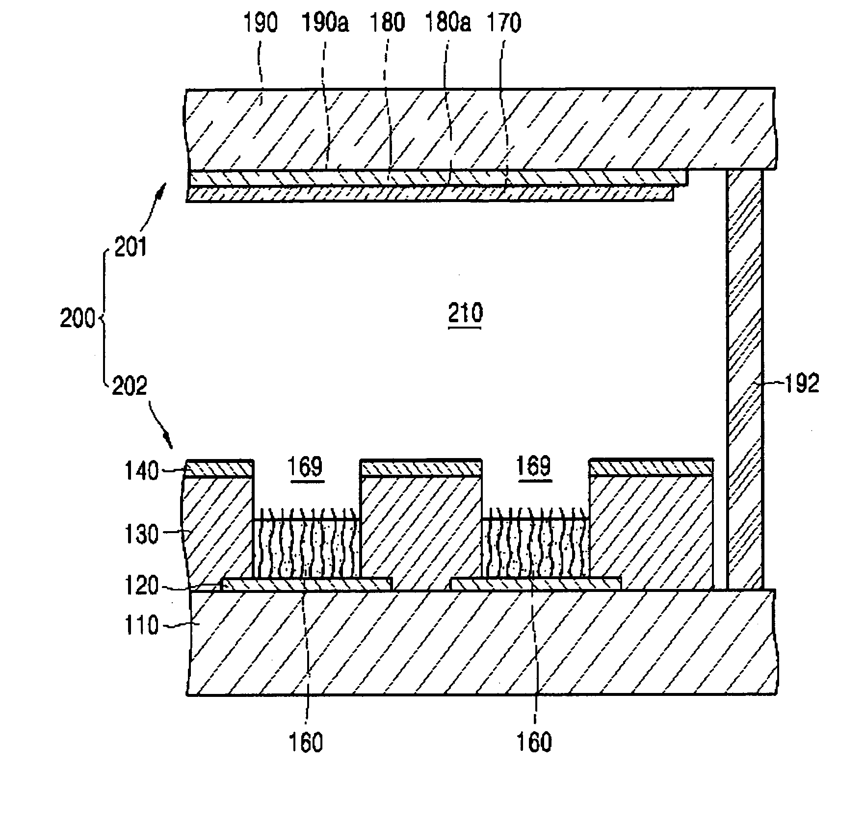
[0063] The composition for forming electron emission sources was applied to an electron emission source regions in a substrate on which Cr gate electrodes, an insulation layer, and ITO electrodes had been formed and exposed to light using a parallel exposure system and a pattern mask at an exposure energy of 2,000 mJ / cm2. After the exposure process, the resulting structure was developed using acetone and heated at 450° C. in the presence of nitrogen gas to obtain electron emission sources.

[0064] Next, a substrate with a phosphor layer and ITO anode thereon was arranged to face the substrate on which the electron emission sources had been formed, and spacers were formed between the two substrates to maintain a constant cell gap, thereby resulting an electron emission ...


PUM

PropertyMeasurementUnit
thicknessaaaaaaaaaa
total thicknessaaaaaaaaaa
temperatureaaaaaaaaaa

Abstract

An electron emission source including a carbon-based material coated with metal carbide in the surface coating layer, of which the metal has a negative Gibbs free energy when forming the metal carbide at 1,500 K or lower, a method of preparing electron emission sources, and an electron emission device including the electron emission source. The electron emission source includes a carbon nanotube coated with metal carbide or a carbon nanotube having a metal carbide layer and a metal coating layer, which are sequentially formed thereon. Thus, the electron emission source has long lifespan without deterioration of electron emitting characteristics. The electron emission source can be used to manufacture electron emission devices with improved reliability.

Description

CLAIM OF PRIORITY [0001] This application claims the priority of Korean Patent Application No. 10-2005-0069639, filed on Jul. 29, 2005, in the Korean Intellectual Property Office, the disclosure of which is incorporated herein in its entirety by reference. BACKGROUND OF THE INVENTION [0002] 1. Field of the Invention [0003] The present invention relates to an electron emission source, a method of preparing the same, and an electron emission device employing the electron emission source, and more particularly, to an electron emission source having long lifespan without reducing current density, a method of preparing the same, and an electron emission device employing the electron emission source to have improved reliability. [0004] 2. Description of the Related Art [0005] An electron emission device includes an anode and a cathode. A voltage is applied between the anode and the cathode to form an electric field. As a result, an electron emission source of the cathode emits electrons. ...

Claims


Application Information

Patent Timeline
Patent Type & Authority Applications(United States)
IPC IPC(8): H01J63/04H01J19/06
CPCB82Y10/00H01J1/304H01J2201/30469H01J31/127H01J9/025B82Y40/00
Inventor CHOI, YOUNG-CHULKIM, JAE-MYUNGKIM, CHANG-WOOKLEE, EUN-MINAM, JOONG-WOOCHO, SUNG-HEEPARK, JONG-HWANIHM, JI-SOON
Owner SAMSUNG SDI CO LTD
Why Eureka
Try Eureka